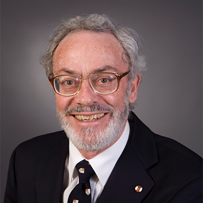
David Lockwood

David Lockwood

The Electrochemical Society values professional and volunteer achievement in the multi-disciplinary sciences. The ECS awards reflect the professional recognition of peers. At meeting plenary sessions, participants from every symposia come together to recognize award winners—some of the greatest minds in the field—and learn about their latest research.

ECS Fellow David J. Lockwood received the Gordon E. Moore Award for Outstanding Achievement in Solid State Science and Technology at the plenary session of the 235th ECS Meeting. This award recognizes outstanding contributions to the fundamental understanding and technological applications of solid state materials, phenomena, and processes. Lockwood is a physicist and researcher emeritus at the National Research Council of Canada. His research centers on the optical properties of low-dimensional materials and focuses on Group IV and III-V semiconductor nanostructures. Lockwood presented “Silicon-Based Photonic Integrated Circuits: The Quest for Compatible Light Sources” at the 235th ECS Meeting Plenary Session. (more…)

The Future of Electronics is Light

By: Arnab Hazari, University of Michigan

ElectronicsFor the past four decades, the electronics industry has been driven by what is called “Moore’s Law,” which is not a law but more an axiom or observation. Effectively, it suggests that the electronic devices double in speed and capability about every two years. And indeed, every year tech companies come up with new, faster, smarter and better gadgets.

Specifically, Moore’s Law, as articulated by Intel cofounder Gordon Moore, is that “The number of transistors incorporated in a chip will approximately double every 24 months.” Transistors, tiny electrical switches, are the fundamental unit that drives all the electronic gadgets we can think of. As they get smaller, they also get faster and consume less electricity to operate.

In the technology world, one of the biggest questions of the 21st century is: How small can we make transistors? If there is a limit to how tiny they can get, we might reach a point at which we can no longer continue to make smaller, more powerful, more efficient devices. It’s an industry with more than US$200 billion in annual revenue in the U.S. alone. Might it stop growing?

Getting close to the limit

At the present, companies like Intel are mass-producing transistors 14 nanometers across – just 14 times wider than DNA molecules. They’re made of silicon, the second-most abundant material on our planet. Silicon’s atomic size is about 0.2 nanometers.

Today’s transistors are about 70 silicon atoms wide, so the possibility of making them even smaller is itself shrinking. We’re getting very close to the limit of how small we can make a transistor.

(more…)

InSe
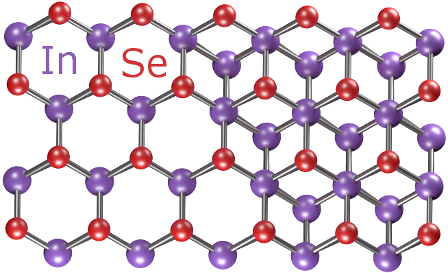
Newly developed semiconductor materials are showing promising potential for the future of super-fast electronics.

A new study out of the University of Manchester details a new material called Indium Selenide (InSe). Like graphene, InSe if just a few atoms thick, but it differs from the “wonder material” in a few critical ways. While graphene has been hailed for its electronic properties, researchers state that it does not have an energy gap – making graphene behave more like a metal than a semiconductor.

Similarly, InSe can be nearly as thin as graphene while exhibiting electronic properties higher than that of silicon. Most importantly, InSe has a large energy gap, which could open the door to super-fast, next-gen electronic devices.

(more…)

The Death of Moore’s Law

The future of technology

The iconic Moore’s law has guided Silicon Valley and the technology industry at large for over 50 years. Moore’s prediction that the number of transistors on a chip would double every two years (which he first articulated at an ECS meeting in 1964) bolstered businesses and the economy, as well as took society away from the giant mainframes of the 1960s to today’s era of portable electronics.

But research has begun to plateau and keeping up with the pace of Moore’s law has proven to be extremely difficult. Now, many tech-based industries find themselves in a vulnerable position, wondering how far we can push technology.

Better materials, better chips

In an effort to continue Moore’s law and produce the next generation of electronic devices, researchers have begun looking to new materials and potentially even new designs to create smaller, cheaper, and faster chips.

“People keep saying of other semiconductors, ‘This will be the material for the next generation of devices,’” says Fan Ren, professor at the University of Florida and technical editor of the ECS Journal of Solid State Science and Technology. “However, it hasn’t really changed. Silicon is still dominating.”

Silicon has facilitated the growth predicted by Moore’s law for the past decades, but it is now becoming much more difficult to continue that path.

(more…)

The iconic Moore’s law has predicted the technological growth of the chip industry for more than 50 years. When ECS member and co-founder of Intel Gordon Moore proposed the law, he stated that the number of transistors on a chip would double every two years. So far, he’s been correct.

But researchers have started hitting an apex that makes keeping the pace of Moore’s law extremely difficult. It has become harder in recent years to make transistors smaller while simultaneously increasing the processing power of chips, making it almost impossible to continue Moore’s law’s projected growth.

However, researchers from MIT have developed a long-awaited tool that may be able to keep driving that progress.

(READ: “Moore’s Law and the Future of Solid-State Electronics“)

The new technology that hopes to keep Moore’s law going at its current pace is called extreme-ultraviolet (EUV) lithography. Industry leaders say it could be used in high-volume chip manufacturing as early as 2018, allowing continued growth in the semiconductor industry, with advancements in our mobile phones, wearable electronics, and many other gadgets.

(more…)

Intel may be known for microprocessors and long-time ECS member Gordon E. Moore, but now the company’s Edison technology is lending itself to something entirely different.

They call it the Spider Dress, and the innovation involved in making this product goes far beyond sheer aesthetic value.

The 3-D printed dress was created by Anouk Wipprecht and uses Intel’s Edison technology to power robotic spider legs surrounding the collar, designed to keep people out of your personal space.

The dress’s robotic arms are connected to proximity sensors, which will react when someone gets too close to the wearer of the dress. Further, the sensors use biometric signals to measure the wearer’s stress level, which allow the dress to respond based on your mood.

(more…)