
Another possibility for this novel technique is to introduce intentionally imperfections into graphene’s lattice structure to create specific mechanical and electronic attributes.
Image: Nature Communications
A new development out of Caltech could be the first step to producing commercially feasible graphene-based solar cells and LEDs, large-panel displays, and flexible electronics.
“With this new technique, we can grow large sheets of electronic-grade graphene in much less time and at much lower temperatures,” says Caltech staff scientist David Boyd, who developed the method.
While the amazing potential of graphene is universally accepted among the scientific community, scientists have struggled with achieving the properties of the material on an industrially relevant level. The existing techniques either require temperatures that are too hot, or have intrinsic flaws such as deformation of the materials that compromise strength properties.
“Previously, people were only able to grow a few square millimeters of high-mobility graphene at a time, and it required very high temperatures, long periods of time, and many steps,” says Caltech physics professor Nai-Chang Yeh, the Fletcher Jones Foundation Co-Director of the Kavli Nanoscience Institute and the corresponding author of the new study.
“Our new method can consistently produce high-mobility and nearly strain-free graphene in a single step in just a few minutes without high temperature. We have created sample sizes of a few square centimeters, and since we think that our method is scalable, we believe that we can grow sheets that are up to several square inches or larger, paving the way to realistic large-scale applications.”
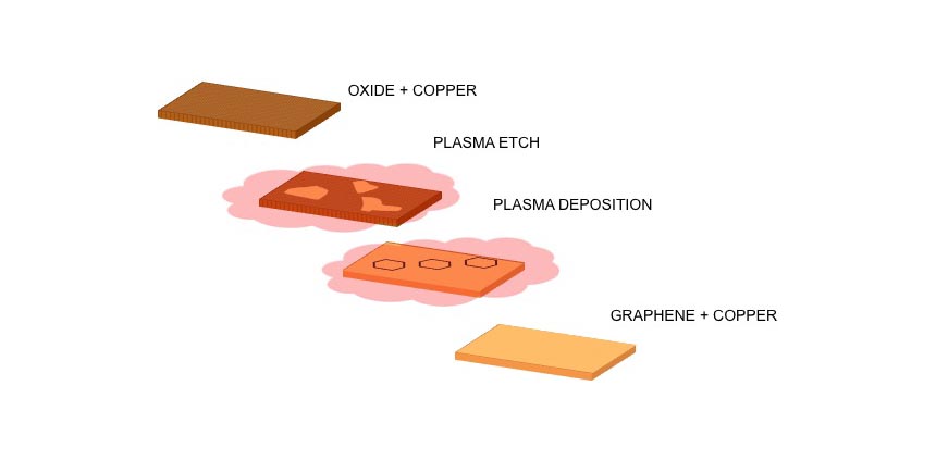
This from Caltech:
The solution Boyd hit upon was to use a system first developed in the 1960s to generate a hydrogen plasma—that is, hydrogen gas that has been electrified to separate the electrons from the protons—to remove the copper oxide at much lower temperatures. His initial experiments revealed not only that the technique worked to remove the copper oxide, but that it simultaneously produced graphene as well.
By producing graphene without extreme heat, manufacturing costs are reduced and the number of potential property defects decline. Also, this new technique will eliminate many post-production steps.
This novel technique will allow for the growth of large sheets of electronic-grade graphene in much less time at much lower temperatures. It could also eventually expand to produce new kinds of electronics manufacturing and sheets used as armor to protect materials against degradation from environmental impact.
The researchers hope that the new development will eventually be able to be used as a transparent conducting electrode for solar cells and display panels.
To learn more about the potential of graphene, check out the papers in the Digital Library. And make sure to take a look at this just-published open access paper on graphene and electrochemical deposition!