Printable Functional Materials

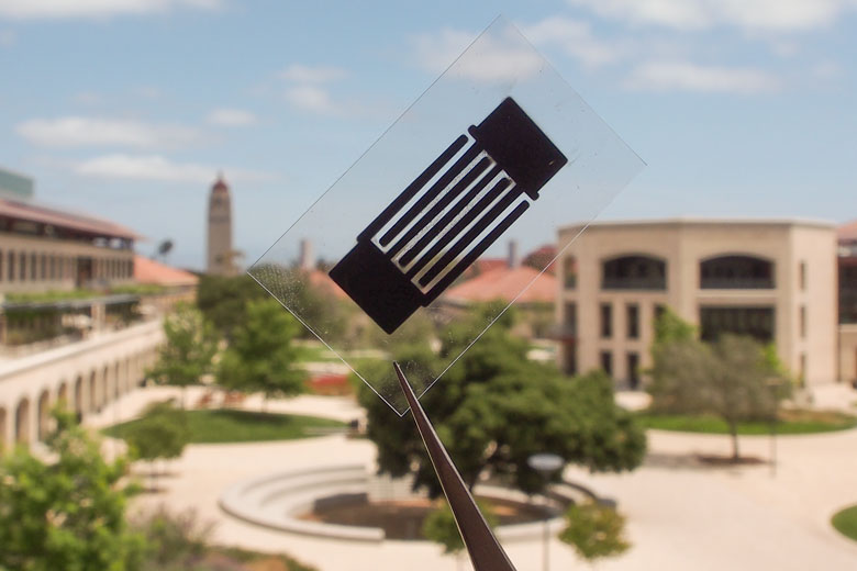
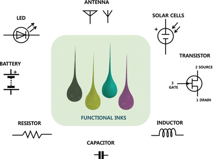
Potential technical applications of printable functional inks.

The video and information in this post relate to an ECS Journal of Solid State Science and Technology focus issue called: Printable Functional Materials for Electronics and Energy Applications.

(Read/download the focus issue now. It’s entirely free.)

Printing technologies in an atmospheric environment offer the potential for low-cost and materials-efficient alternatives for manufacturing electronics and energy devices such as luminescent displays, thin-film transistors, sensors, thin-film photovoltaics, fuel cells, capacitors, and batteries. Significant progress has been made in the area of printable functional organic and inorganic materials including conductors, semiconductors, and dielectric and luminescent materials.

These new printable functional materials have and will continue to enable exciting advances in printed electronics and energy devices. Some examples are printed amorphous oxide semiconductors, organic conductors and semiconductors, inorganic semiconductor nanomaterials, silicon, chalcogenide semiconductors, ceramics, metals, intercalation compounds, and carbon-based materials.

A special focus issue of the ECS Journal of Solid State Science and Technology was created about the publication of state-of-the-art efforts that address a variety of approaches to printable functional materials and device. This focus issue, consisting of a total of 15 papers, includes both invited and contributed papers reflecting recent achievements in printable functional materials and devices.

The topics of these papers span several key ECS technical areas, including batteries, sensors, fuel cells, carbon nanostructures and devices, electronic and photonic devices, and display materials, devices, and processing. The overall collection of this focus issue covers an impressive scope from fundamental science and engineering of printing process, ink chemistry and ink conversion processes, printed devices, and characterizations to the future outlook for printable functional materials and devices.

The video below show demonstrates Inkjet Printed Conductive Tracks for Printed Electronic conducted by S.-P. Chen, H.-L. Chiu, P.-H. Wang, and Y.-C. Liao, Department of Chemical Engineering, National Taiwan University, No. 1 Sec. 4 Roosevelt Road, Taipei 10617, Taiwan.

Step-by-step explanation of the video:

For printed electronic devices, metal thin film patterns with great conductivities are required. Three major ways to produce inkjet-printed metal tracks will be shown in this video.

(more…)

The "designer carbon" improved the supercapacitor's electrical conductivity threefold compared to electrodes made of conventional activated carbon.Image: Stanford University

The “designer carbon” improved the supercapacitor’s electrical conductivity threefold compared to electrodes made of conventional activated carbon.
Image: Stanford University

Stanford University researchers have developed a new “designer carbon” that can be fine-tuned for a variety of applications, including energy storage and water filters.

The newly developed carbon material has shown that it can significantly improve the power delivery rate of supercapacitors and boost the performance of energy storage technologies.

“We have developed a ‘designer carbon’ that is both versatile and controllable,” said Zhenan Bao, past member of ECS and the senior author of the study. “Our study shows that this material has exceptional energy-storage capacity, enabling unprecedented performance in lithium-sulfur batteries and supercapacitors.”

(PS: Check out some of Bao’s past papers in the Digital Library!)

Not only is the new carbon an improvement over existing versions, it also has a huge potential scope and is inexpensive to produce.

(more…)

Three Atom Thick Transistor

A new study by two ECS published authors, David Muller and Jiwoong Park, has led to an electronic piece that is just three atoms thick.

The researchers have unveiled a process to develop ultra-thin transistors made from TMD, otherwise known as transition metal dichalcogenide. This material is novel in the fact that it possesses properties that make it a perfect fit for solar cells, light detectors, or semiconductors.

Researchers have been examining TMDs for some time now, but have been finding it difficult to get them to work consistently. This new study has discovered the best process yet to manufacture the materials, which could lead to a breakthrough in the future of electronics and possibly bring about an end to Moore’s law.

(more…)

First Ever Liquid Nanoscale Laser

The laser also has the potential to be used in optical data storage and lithography.Image: Nature Communications

The laser also has the potential to be used in optical data storage and lithography.
Image: Nature Communications

Former ECS member Teri Odom has assisted in the development of the first ever liquid nanoscale laser. This development could lead to some very practical applications, as well as guiding researchers one step closer to developing a “lab on a chip” for medical diagnostics.

The laser is relatively simple to create, cheap to produce, and has the ability to operate at room temperature. Because the device works in real time, users can quickly and simply produce different colors.

This from Science World Report:

The laser’s cavity itself is made up of an array of reflective gold nanoparticles where the light is concentrated around each nanoparticle and then amplified. In contrast to conventional laser cavities, no mirrors are required for the light to bounce back and forth. As the laser color is tuned the nanoparticle cavity stays fixed and does not change.

(more…)

Water Helps Form Tiniest Wires Ever

The nanowires were created through a process called meniscus-mask lithography.Image: Tour Group/Rice University

The nanowires were created through a process called meniscus-mask lithography.
Image: Tour Group/Rice University

Scientists and researchers around the world are always looking for ways to improve technology. While we’ve been making smaller circuits to improve semiconductors for some time now, we’ve just about reached the physical limits of shrinking nanowires. However, this newly developed technique allows for the formation of the tiniest wires yet.

A new technique has been developed that uses water to create patterns of wires less than 10 nanometers wide.

“This could have huge ramifications for chip production since the wires are easily made to sub-10-nanometer sizes,” said lead author James M. Tour. “There’s no other way in the world to do this en masse on a surface.”

(more…)

  • Page 5 of 5