By: Peter Byrley, University of California, Riverside

A smartphone touchscreen is an impressive piece of technology. It displays information and responds to a user’s touch. But as many people know, it’s easy to break key elements of the transparent, electrically conductive layers that make up even the sturdiest rigid touchscreen. If flexible smartphones, e-paper and a new generation of smart watches are to succeed, they can’t use existing touchscreen technology.

We’ll need to invent something new – something flexible and durable, in addition to being clear, lightweight, electrically responsive and inexpensive. Many researchers are pursuing potential options. As a graduate researcher at the University of California, Riverside, I’m part of a research group working to solve this challenge by weaving mesh layers out of microscopic strands of metal – building what we call metal nanowire networks.

These could form key components of new display systems; they could also make existing smartphones’ touchscreens even faster and easier to use.

The problem with indium tin oxide

A standard smartphone touchscreen has glass on the outside, on top of two layers of conductive material called indium tin oxide. These layers are very thin, transparent to light and conduct small amounts of electrical current. The display lies underneath.

When a person touches the screen, the pressure of their finger bends the glass very slightly, pushing the two layers of indium tin oxide closer together. In resistive touchscreens, that changes the electrical resistance of the layers; in capacitive touchscreens, the pressure creates an electrical circuit.

(more…)

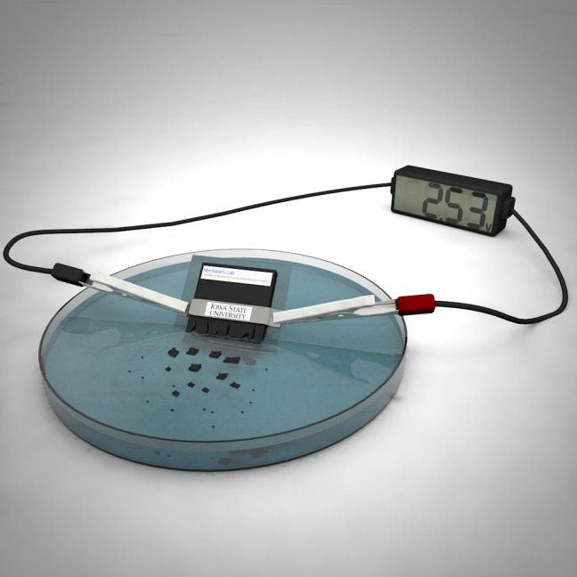
Researchers have created a flexible electronic device that can easily degrade just by adding a weak acid like vinegar.

“In my group, we have been trying to mimic the function of human skin to think about how to develop future electronic devices,” says Stanford University engineer Zhenan Bao.

She described how skin is stretchable, self-healable, and also biodegradable—an attractive list of characteristics for electronics. “We have achieved the first two [flexible and self-healing], so the biodegradability was something we wanted to tackle.”

A United Nations Environment Program report found that almost 50 million tons of electronic waste were thrown out in 2017—more than 20 percent higher than waste in 2015.

“This is the first example of a semiconductive polymer that can decompose,” says lead author Ting Lei, a postdoctoral fellow working with Bao.

In addition to the polymer—essentially a flexible, conductive plastic—the team developed a degradable electronic circuit and a new biodegradable substrate material for mounting the electrical components. This substrate supports the electrical components, flexing and molding to rough and smooth surfaces alike. When the electronic device is no longer needed, the whole thing can biodegrade into nontoxic components.

(more…)

Posted in Technology

Two discoveries could provide a simple and effective way to “stencil” high-quality 2D materials in precise locations and overcome a barrier to their use in next-generation electronics.

In 2004, the discovery of a way to isolate a single atomic layer of carbon—graphene —opened a new world of 2D materials with properties not necessarily found in the familiar 3D world. Among these materials are a large group of elements—transition metals—that fall in the middle of the periodic table.

When atoms of certain transition metals, for instance molybdenum, are layered between two layers of atoms from the chalcogenide elements, such as sulfur or selenium, the result is a three-layer sandwich called a transition metal dichalcogenide. TMDs have created tremendous interest among materials scientists because of their potential for new types of electronics, optoelectronics and computation.

“What we have focused on in this paper is the ability to make these materials over large areas of a substrate in precisely the places we want them,” says Joshua Robinson, associate professor of materials science and engineering at Penn State. “These materials are of interest for a variety of next-generation electronics, not necessarily to replace silicon, but to augment current technologies and ultimately to bring new chip functionality to silicon that we never had before.”

(more…)

ElectronicsNew research demonstrates the development of the first stretchable integrated circuit, made entirely using an inkjet printer.

The team behind this research believes this development could lead to the manufacturing of inexpensive “smart fabric.” Potential applications include wallpaper that can turn an entire wall into an electronic display and electronics that could be scaled up and down easily.

“We can conceivably make the costs of producing flexible electronics comparable to the costs of printing newspapers,” says Chuan Wang, co-author of the paper and former ECS member. “Our work could soon lead to printed displays that can easily be stretched to larger sizes, as well as wearable electronics and soft robotics applications.”

(more…)

Nano-chimney to Cool Circuits

Overheating has emerged as a primary concern in the development of new electronic devices. A new study from Rice University looks to provide a solution to that, offering a strategy to vent heat away from nano-electronics through cone-like chimneys.

By putting these “chimneys” between the graphene and nanotube, the researchers effectively eliminate a barrier that typically blocks heat from escaping.

This from Rice University:

Researchers at Rice University discovered through computer simulations that removing atoms here and there from the two-dimensional graphene base would force a cone to form between the graphene and the nanotube. The geometric properties of the graphene-to-cone and cone-to-nanotube transitions require the same total number of heptagons, but they are more sparsely spaced and leave a clear path of hexagons available for heat to race up the chimney.

(more…)

The Future of Electronics is Light

By: Arnab Hazari, University of Michigan

ElectronicsFor the past four decades, the electronics industry has been driven by what is called “Moore’s Law,” which is not a law but more an axiom or observation. Effectively, it suggests that the electronic devices double in speed and capability about every two years. And indeed, every year tech companies come up with new, faster, smarter and better gadgets.

Specifically, Moore’s Law, as articulated by Intel cofounder Gordon Moore, is that “The number of transistors incorporated in a chip will approximately double every 24 months.” Transistors, tiny electrical switches, are the fundamental unit that drives all the electronic gadgets we can think of. As they get smaller, they also get faster and consume less electricity to operate.

In the technology world, one of the biggest questions of the 21st century is: How small can we make transistors? If there is a limit to how tiny they can get, we might reach a point at which we can no longer continue to make smaller, more powerful, more efficient devices. It’s an industry with more than US$200 billion in annual revenue in the U.S. alone. Might it stop growing?

Getting close to the limit

At the present, companies like Intel are mass-producing transistors 14 nanometers across – just 14 times wider than DNA molecules. They’re made of silicon, the second-most abundant material on our planet. Silicon’s atomic size is about 0.2 nanometers.

Today’s transistors are about 70 silicon atoms wide, so the possibility of making them even smaller is itself shrinking. We’re getting very close to the limit of how small we can make a transistor.

(more…)

InSeNewly developed semiconductor materials are showing promising potential for the future of super-fast electronics.

A new study out of the University of Manchester details a new material called Indium Selenide (InSe). Like graphene, InSe if just a few atoms thick, but it differs from the “wonder material” in a few critical ways. While graphene has been hailed for its electronic properties, researchers state that it does not have an energy gap – making graphene behave more like a metal than a semiconductor.

Similarly, InSe can be nearly as thin as graphene while exhibiting electronic properties higher than that of silicon. Most importantly, InSe has a large energy gap, which could open the door to super-fast, next-gen electronic devices.

(more…)

Biomedical innovations have helped shape the world of modern medicine. From pacemakers to auto-dispensing medications, advances in medical technology have revolutionized the world we live in.

But what happens when some of these devices need to be removed?

That’s where “transient electronics” come in. The concept behind this new technology is that rather than removing medical devices through surgery, scientists could simply develop the device so it could just disappear when the time is appropriate.

The latest development in transient electronics comes from Iowa State University, where researchers have made a breakthrough in the development of a dissolving battery that could power these disappearing devices.

The lithium-ion battery can deliver 2.5 volts and dissipate in 30 minutes when dropped into water. The power generated from the battery could power a desktop calculator for about 15 minutes.

(more…)

Posted in Technology

From televisions screens we can roll up like newspapers to see-through batteries, researchers are moving electronics toward a more flexible, more transparent future.

The most recent development in this area comes from a group that has developed transparent, flexible supercapacitors made of carbon nanotube films. But this development goes far beyond wearable electronics, with potential applications in both energy storage and harvesting.

“Potential applications can be roughly divided into two categories: high-aesthetic-value products, such as activity bands and smart clothes, and inherently transparent end-uses, such as displays and windows,” co-author of the study Tanja Kallio, told Phys.org. “The latter include, for example, such future applications as smart windows for automobiles and aerospace vehicles, self-powered rolled-up displays, self-powered wearable optoelectronics, and electronic skin.”

With the thin films demonstrating 92 percent transparency and high efficiency compared to other carbon-based counterparts, the researchers believe that further improvements to the supercapacitors durability and energy density could make the product commercially viable.

The Death of Moore’s Law

The future of technology

The iconic Moore’s law has guided Silicon Valley and the technology industry at large for over 50 years. Moore’s prediction that the number of transistors on a chip would double every two years (which he first articulated at an ECS meeting in 1964) bolstered businesses and the economy, as well as took society away from the giant mainframes of the 1960s to today’s era of portable electronics.

But research has begun to plateau and keeping up with the pace of Moore’s law has proven to be extremely difficult. Now, many tech-based industries find themselves in a vulnerable position, wondering how far we can push technology.

Better materials, better chips

In an effort to continue Moore’s law and produce the next generation of electronic devices, researchers have begun looking to new materials and potentially even new designs to create smaller, cheaper, and faster chips.

“People keep saying of other semiconductors, ‘This will be the material for the next generation of devices,’” says Fan Ren, professor at the University of Florida and technical editor of the ECS Journal of Solid State Science and Technology. “However, it hasn’t really changed. Silicon is still dominating.”

Silicon has facilitated the growth predicted by Moore’s law for the past decades, but it is now becoming much more difficult to continue that path.

(more…)

  • Page 2 of 4