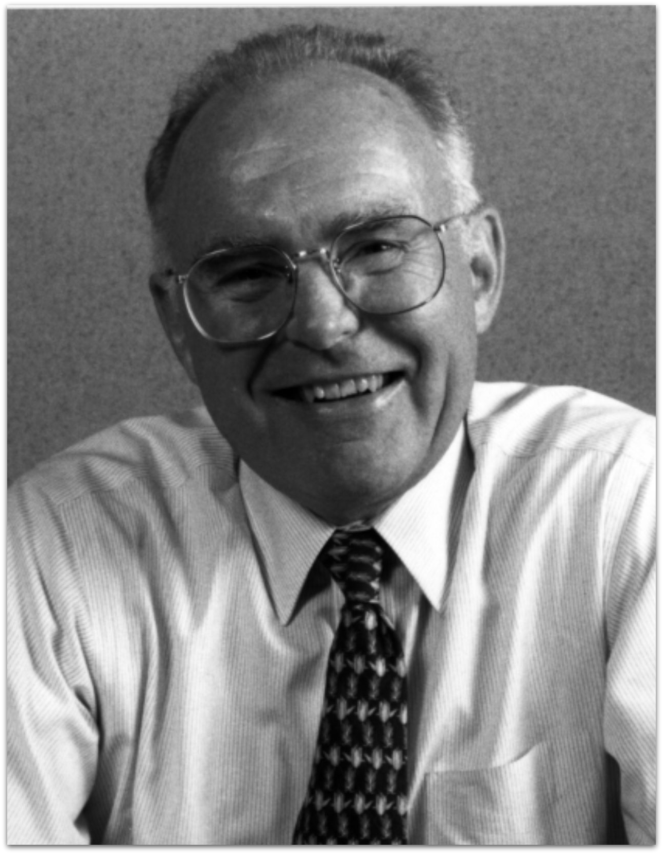
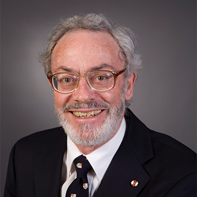
David Lockwood

David Lockwood

The Electrochemical Society values professional and volunteer achievement in the multi-disciplinary sciences. The ECS awards reflect the professional recognition of peers. At meeting plenary sessions, participants from every symposia come together to recognize award winners—some of the greatest minds in the field—and learn about their latest research.

ECS Fellow David J. Lockwood received the Gordon E. Moore Award for Outstanding Achievement in Solid State Science and Technology at the plenary session of the 235th ECS Meeting. This award recognizes outstanding contributions to the fundamental understanding and technological applications of solid state materials, phenomena, and processes. Lockwood is a physicist and researcher emeritus at the National Research Council of Canada. His research centers on the optical properties of low-dimensional materials and focuses on Group IV and III-V semiconductor nanostructures. Lockwood presented “Silicon-Based Photonic Integrated Circuits: The Quest for Compatible Light Sources” at the 235th ECS Meeting Plenary Session. (more…)

Gordon Moore, Interface
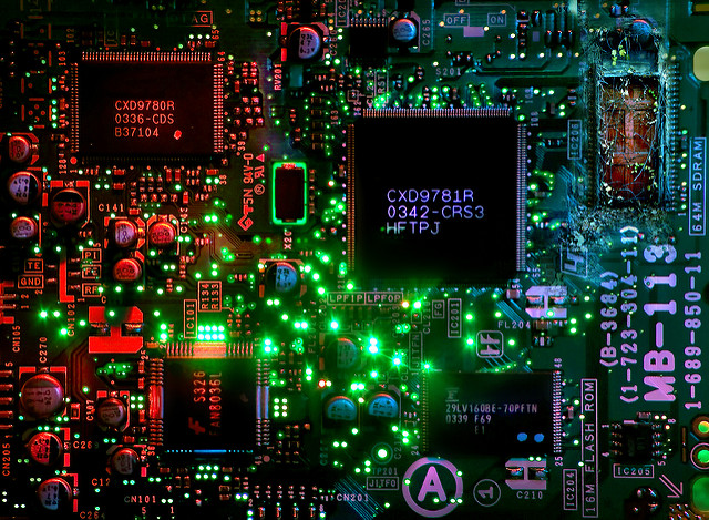
Nineteen sixty-eight marked a year of tragedy but also of transformation. It may be 50 years in our past, but what occurred that year is still very much alive with us today. Here are our top 5 reasons why the scientific advances of that year are super “groovy” in our book:

5. Patent for the jacuzzi whirlpool hot tub granted

Roy Jacuzzi realized early on that the market for leisure and fitness was a growing one. He set out to create a bathtub that allowed enough room to offer “a relaxing soak,” according to Jacuzzi Inc.’s company history page. With that, the first bathtub with a built-in whirlpool system was born. The laid-back culture of California in the 1970s turned out to be the perfect launching ground for the now widely appreciated and known jacuzzi.

4. Apollo 8 is the first manned spacecraft to orbit the moon

Jim Lovell, Bill Anders, and Frank Borman became the first human beings to orbit another world. According to NASA, on Christmas Eve 1968 the three men were the first to orbit the moon and see  Earth as a whole planet. With that, Jim Lovell confirmed, “there is a Santa Claus.”

(more…)

Making the New Silicon

Shown here is the smallest laptop power adapter ever, made using GaN transistors.
Image: Cambridge Electronics

Recent discussions in the electronics industry have revolved around the future of technology in light of the perceived end of Moore’s law. But what if the iconic law doesn’t have to end? Researchers from MIT believe they have exactly what it takes to keep up with the constantly accelerating pace of Moore’s law.

More efficient materials

For the scientists, the trick is in the utilization of a material other than silicon in semiconductors for power electronics. With extremely high efficiency levels that could potentially reduce worldwide energy consumption, some believe that material could be gallium nitride (GaN).

MIT spin-out Cambridge Electronics Inc. (CEI) has recently produced a line of GaN transistors and power electronic circuits. The goal is to cut energy usage in data centers, electric cars, and consumer devices by 10 to 20 percent worldwide by 2025.

Semiconductors shaping society

Since its discovery in 1947, the transistor has helped make possible many wonders of modern life – including smartphones, solar cells, and even airplanes.

Over time, as predicted by Moore’s law, transistors became smaller and more efficient at an accelerated pace – opening doors to even more technological advancements.

(more…)

The Death of Moore’s Law

The future of technology

The iconic Moore’s law has guided Silicon Valley and the technology industry at large for over 50 years. Moore’s prediction that the number of transistors on a chip would double every two years (which he first articulated at an ECS meeting in 1964) bolstered businesses and the economy, as well as took society away from the giant mainframes of the 1960s to today’s era of portable electronics.

But research has begun to plateau and keeping up with the pace of Moore’s law has proven to be extremely difficult. Now, many tech-based industries find themselves in a vulnerable position, wondering how far we can push technology.

Better materials, better chips

In an effort to continue Moore’s law and produce the next generation of electronic devices, researchers have begun looking to new materials and potentially even new designs to create smaller, cheaper, and faster chips.

“People keep saying of other semiconductors, ‘This will be the material for the next generation of devices,’” says Fan Ren, professor at the University of Florida and technical editor of the ECS Journal of Solid State Science and Technology. “However, it hasn’t really changed. Silicon is still dominating.”

Silicon has facilitated the growth predicted by Moore’s law for the past decades, but it is now becoming much more difficult to continue that path.

(more…)

The iconic Moore’s law has predicted the technological growth of the chip industry for more than 50 years. When ECS member and co-founder of Intel Gordon Moore proposed the law, he stated that the number of transistors on a chip would double every two years. So far, he’s been correct.

But researchers have started hitting an apex that makes keeping the pace of Moore’s law extremely difficult. It has become harder in recent years to make transistors smaller while simultaneously increasing the processing power of chips, making it almost impossible to continue Moore’s law’s projected growth.

However, researchers from MIT have developed a long-awaited tool that may be able to keep driving that progress.

(READ: “Moore’s Law and the Future of Solid-State Electronics“)

The new technology that hopes to keep Moore’s law going at its current pace is called extreme-ultraviolet (EUV) lithography. Industry leaders say it could be used in high-volume chip manufacturing as early as 2018, allowing continued growth in the semiconductor industry, with advancements in our mobile phones, wearable electronics, and many other gadgets.

(more…)

IBM’s New Chip Quadruples Capacity

In recent years, the semiconductor industry has struggled to keep up with the pace of the legendary Moore’s Law. With the current 14-nanometer generation of chips, researchers have begun to question if it will remain possible to double transistor density every two and a half years. However, IBM is now pushing away the doubt with the development of their new chip.

The new ultra-dense chip hosts seven-nanometer transistors, which yields about four times the capacity of our current computer chip. Like many other researchers in the field, IBM decided to move away for the traditional and expensive pure silicon toward a silicon-germanium hybrid material to produce the new chip.

The success of the high-capacity chip relies on the utilization of this new material. The use of silicon-germanium has made it possible for faster transistor switching and lower power requirements. And did we mention how impossibly small these transistors are?

(more…)

50 Years of Moore’s Law

mooreThe iconic Moore’s Law will mark its 50th anniversary this Sunday, April 19th. In celebration, we’ll be taking a look at the solid state revolutionary who made the incredible prediction, the inception of the law, and the deep-rooted links between Gordon Moore and The Electrochemical Society.

The initial transformation in the electronics industry began with an invention at Bell Labs in late 1947 of a little device known as the transistor. The transistor acted as a catalyst of change not only for solid state science and the electronics industry, but also for the composition and spirit of ECS membership—which would begin to be centered on the Electronics Division.

Prior to this solid state surge, electronics—specifically the Electronics Division at ECS—was centered on topics such as phosphors and cathode ray tubes in light of the advent of television. Moore joined ECS in 1957 and helped transform the division into something new—something exciting.

(more…)

Intel may be known for microprocessors and long-time ECS member Gordon E. Moore, but now the company’s Edison technology is lending itself to something entirely different.

They call it the Spider Dress, and the innovation involved in making this product goes far beyond sheer aesthetic value.

The 3-D printed dress was created by Anouk Wipprecht and uses Intel’s Edison technology to power robotic spider legs surrounding the collar, designed to keep people out of your personal space.

The dress’s robotic arms are connected to proximity sensors, which will react when someone gets too close to the wearer of the dress. Further, the sensors use biometric signals to measure the wearer’s stress level, which allow the dress to respond based on your mood.

(more…)

ECS history book cover

Created for the centennial celebration of The Electrochemical Society (1902-2002).

Since its foundation in 1902, ECS and its members have been at the forefront of the challenge to bridge the gap between electrical engineering and chemistry. The years that followed the Society’s establishment have been filled with innovation, ingenuity, and excellence throughout the field of electrochemistry. Take a look back at some of ECS’s most prestigious members and their accomplishments.

Samuel Ruben

Ruben presenting his Acheson Award address in 1970.

Samuel Ruben
In 1918, Samuel Ruben, an 18-year old high school graduate, was hired by the Electrochemical Products Company in New York City. Bergen Davis of Columbia University arranged for Ruben to sit in on courses at Columbia and spent evenings tutoring him. Ruben went on to invent the dry electrolytic aluminum capacitor, the vacuum tube relay, the quick heather vacuum tube, a sold-state rectifier, and the balanced cell mercury battery.

(more…)