By: Elton Santos, Queen’s University Belfast

CarbonScientists have found a way to make carbon both very hard and very stretchy by heating it under high pressure. This “compressed glassy carbon”, developed by researchers in China and the US, is also lightweight and could potentially be made in very large quantities. This means it might be a good fit for several sorts of applications, from bulletproof vests to new kinds of electronic devices.

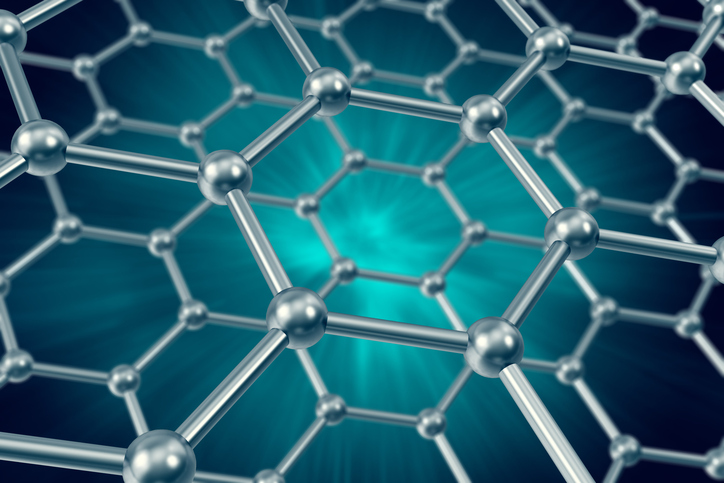
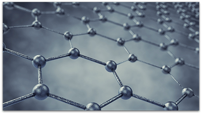
Carbon is a special element because of the way its atoms can form different types of bonds with each other and so form different structures. For example, carbon atoms joined entirely by “sp³” bonds produce diamond, and those joined entirely by “sp²” bonds produce graphite, which can also be separated into single layers of atoms known as graphene. Another form of carbon, known as glassy carbon, is also made from sp² and has properties of both graphite and ceramics.

But the new compressed glassy carbon has a mix of sp³ and sp² bonds, which is what gives it its unusual properties. To make atomic bonds you need some additional energy. When the researchers squeezed several sheets of graphene together at high temperatures, they found certain carbon atoms were exactly in the right position to form sp³ bonds between the layers.

By studying the new material in detail, they found that just over one in five of all its bonds were sp³. This means that most of the atoms are still arranged in a graphene-like structure, but the new bonds make it look more like a large, interconnected network and give it greater strength. Over the small scale of individual graphene sheets, the atoms are arranged in an orderly, hexagonal pattern. But on a larger scale, the sheets are arranged in a disorderly fashion. This is probably what gives it the combined properties of hardness and flexibility.

(more…)

GrapheneA quantum probe based on an atomic-sized “color center” in diamonds has let researchers observe the flow of electric currents in graphene.

Made up of a lattice of carbon atoms only one atom thick, graphene is a key material for the electronics of the future. The thin carbon material is stronger than steel and due to its flexibility, transparency, and ability to conduct electricity, holds great promise for use in solar cells, touch panels, and flexible electronics.

No one has been able to see what is happening with electronic currents in graphene, says Lloyd Hollenberg, professor at the University of Melbourne and deputy director of the Centre for Quantum Computation and Communication Technology.

According to Hollenberg, this new technique overcomes significant limitations with existing methods for understanding electric currents in devices based on ultra-thin materials.

(more…)

Two discoveries could provide a simple and effective way to “stencil” high-quality 2D materials in precise locations and overcome a barrier to their use in next-generation electronics.

In 2004, the discovery of a way to isolate a single atomic layer of carbon—graphene —opened a new world of 2D materials with properties not necessarily found in the familiar 3D world. Among these materials are a large group of elements—transition metals—that fall in the middle of the periodic table.

When atoms of certain transition metals, for instance molybdenum, are layered between two layers of atoms from the chalcogenide elements, such as sulfur or selenium, the result is a three-layer sandwich called a transition metal dichalcogenide. TMDs have created tremendous interest among materials scientists because of their potential for new types of electronics, optoelectronics and computation.

“What we have focused on in this paper is the ability to make these materials over large areas of a substrate in precisely the places we want them,” says Joshua Robinson, associate professor of materials science and engineering at Penn State. “These materials are of interest for a variety of next-generation electronics, not necessarily to replace silicon, but to augment current technologies and ultimately to bring new chip functionality to silicon that we never had before.”

(more…)

From artificial limbs to cochlear implants, biomedical advancements are opening up new opportunities for health care. Now, researchers from the University of Delaware are working to further improve the lifetime and effectiveness of those biomedical devices by improving communication between the technology and neural tissue.

In order to improve the devices, researchers worked to develop a direct interfacing material to improve communication between the device and the body. For this, the team focused on a conjugated polymer known as PEDOT.

Video credit: Leah Dodd/ University of Delaware

This from University of Delaware:

Compared to other methods, surface modification through electro-grafting takes just minutes. Another advantage is that a variety of materials can be used as the conducting substrate, including gold, platinum, glassy carbon, stainless steel, nickel, silicon, and metal oxides.

Read the full article.

“Our results suggest that this is an effective means to selectively modify microelectrodes with highly adherent and highly conductive polymer coatings as direct neural interfaces,” says David Martin, lead researcher.

By: Mike Williams, Rice University

Graphene
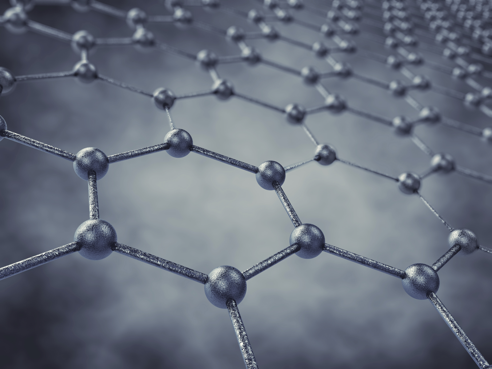
A new type of conductive graphene foam is incredibly tough and can be formed into just about any shape and size.

A chunk of the foam, which is reinforced by carbon nanotubes, can support more than 3,000 times its own weight and easily bounce back to its original height.

The Rice University lab of chemist James Tour tested this new “rebar graphene” as a highly porous, conductive electrode in lithium ion capacitors and found it to be mechanically and chemically stable. The results appear in the journal ACS Applied Materials and Interfaces.

Carbon in the form of atom-thin graphene is among the strongest materials known and is highly conductive; multiwalled carbon nanotubes are widely used as conductive reinforcements in metals, polymers and carbon matrix composites. The Tour lab had already used nanotubes to reinforce two-dimensional sheets of graphene. Extending the concept to macroscale materials made sense, says Tour, a professor of computer science and of materials science and nanoengineering.

“We developed graphene foam, but it wasn’t tough enough for the kind of applications we had in mind, so using carbon nanotubes to reinforce it was a natural next step,” Tour adds.

(more…)

Achieving a More Efficient Catalyst

Nanoporous goldA new study out of Lawrence Livermore National Laboratory shows that catalysts derived from nano-structured materials are as good as gold.

According to the study, led by past ECS member Juergen Biener, restructuring nanoporous gold alloys result in more efficient catalysts.

Nano-structured materials have shown promising qualities for improving catalyst activity and selectivity, but little is known about the structural changes that the materials undergo that can create or prevent efficient catalyst function.

This from LLNL:

The team used ozone-activated silver-gold alloys in the form of nanoporous gold (npAu) as a case study to demonstrate the dynamic behavior of bi-metallic systems during activation to produce a functioning catalyst. Nanoporous gold, a porous metal, can be used in electrochemical sensors, catalytic platforms, fundamental structure property studies at the nanoscale and tunable drug release. It also features high effective surface area, tunable pore size, well-defined conjugate chemistry, high electrical conductivity and compatibility with traditional fabrication techniques.

(more…)

New research out of the University of California, Riverside reveals a transparent, self-healing, highly stretchable material that can be electrically activated to power artificial muscles or improve batteries and electronic devices.

The researchers behind the development believe that this new material could be used to extend the lifetime of lithium-ion batteries in electric vehicles, improve medical and environmental biosensors, and even allow robots to self-heal after mechanical failure.

“Creating a material with all these properties has been a puzzle for years,” says Chao Wang, co-author of the recently published research. “We did that and now are just beginning to explore the applications.”

According to the research, the low-cost material can stretch 50 times its original length and can complete heal in 24 hours after being cut.

Silly putty isn’t just for kids anymore.

Researchers in Ireland combined the classic kid’s toy with a special form of carbon to create a new material that has potential applications in medical devices such as heart monitors.


About 70 years ago, scientists came up with the recipe for silly putty as a substitute for rubber. The resulting formula yielded strange properties, but not many applications. However, by taking the strange silly putty formula and mixing it with graphene, the new mixture showed remarkable electrical, bouncy, liquid-like properties.

GrapheneResearchers are shedding new light on cell biology with the development of a graphene sensor to monitor changes in the mitochondria.

The one-atom-thin layer of carbon sensor is giving researchers a new outlook into the process known as programmed cell death in mitochondria. The mitochondrion, which is found in most cells, has been known as the powerhouse of the cell due to its ability to metabolize and create energy for cells. However, the new researcher out of University of California, Irving shows that that convention wisdom on how cells create energy is only half right.

This from UC Irving:

[Peter] Burke and his colleagues tethered about 10,000 purified mitochondria, separated from their cells, to a graphene sensor via antibodies capable of recognizing a protein in their outer membranes. The graphene’s qualities allowed it to function as a dual-mode sensor; its exceptional electrical sensitivity let researchers gauge fluctuations in the acidity levels surrounding the mitochondria, while its optical transparency enabled the use of fluorescent dyes for the staining and visualization of voltage across the inner mitochondrial membranes.

(more…)

GrapheneOver the past few years, researchers have been exploring graphene’s amazing properties and vast potential applications. Now, a team from Iowa State University is looking to take those properties enabled by graphene and applied them to sensors and other technologies.

Many scientists have had a hard time moving graphene from the lab to the marketplace, but the research team from Iowa State University saw potential in using inkjet printers to create multi-layer graphene circuits and electrodes for the production of flexible, wearable electronics.

“Could we make graphene at scales large enough for glucose sensors?” ECS member and Iowa State University postdoctoral researcher, Suprem Das, wanted to know.

(MORE: Read more of Das’ work in the ECS Digital Library.)

The problem with the printing process is that the graphene would then have to be treated to improve its electrical conductivity, which could degrade the flexibility. Instead of using high temperatures and chemical to do this treatment, Das and other members of the team opted to use lasers.

(more…)

  • Page 3 of 8