Layers of Logic Produce Skyscraper Chips

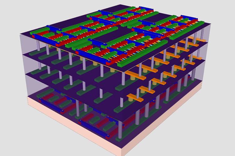
Stanford engineers have created a four-layer prototype high-rise chip. The bottom and top layers are transistors, which are sandwiched between two layers of memory.
Credit: Max Shulaker, Stanford

Cheaper, smaller, and faster – those are the three words we’re constantly hearing when it comes to innovation and development in electronics. Now, Stanford University engineers are adding a fourth word to that mantra – taller.

The Stanford team is about to reveal how to build a high-rise chip that could vault the performance of the single-story logic and memory chips on today’s circuit cards – thereby preventing the wires connecting logic and memory from jamming.

This from Stanford University:

The Stanford approach would end these jams by building layers of logic atop layers of memory to create a tightly interconnected high-rise chip. Many thousands of nanoscale electronic “elevators” would move data between the layers much faster, using less electricity, than the bottleneck-prone wires connecting single-story logic and memory chips today.

(more…)

New Sensor Can Improve the Taste of Your Wine

PhD student Joana Guerreiro has taken part in developing a sensor, which has been dubbed the 'mini-mouth'.Credit: Lars Kruse, Aarhus University

PhD student Joana Guerreiro has taken part in developing a sensor, which has been dubbed the ‘mini-mouth’.
Credit: Lars Kruse, Aarhus University

The ‘mini-mouth’ – that’s what scientists have dubbed the new nanosensor that can mimic the sensation that wine creates in a person’s mouth, which then determines how a specific alcohol tastes.

This technology was created by PhD student Joana Guerreiro from Aarhus University in Denmark, and sets out to detect the level of astringency associated with a particular wine. A wine’s astringency is characterized by the dry sensation drinkers get in their mouth when they drink wine.

This from Aarhus University:

Quite specifically, the sensor is a small plate coated with nanoscale gold particles. On this plate, the researchers simulate what happens in your mouth by first adding some of the proteins contained in your saliva. After this they add the wine. The gold particles on the plate act as nano-optics and make it possible to focus a beam of light below the diffraction limit so as to precisely measure something that is very small – right down to 20 nanometres. This makes it possible to study and follow the proteins, and to see what effect the wine has. It is thereby possible to see the extent to which the small molecules have to bind together for the clumping effect on the protein to be set off.

Read the full article here.

While the technique itself is not new, the ingenuity lies in using it to create a sensor that can measure an effect rather than just the number of molecules.

This technology seems as though it would threaten the livelihood of sommeliers, but researchers say that is not what the sensor is intended for. Instead, the team at Aarhus University hopes that this will produce a tool that is useful in wine production.

Want to see what else sensors can do? Head over to our Digital Library to see the newest cutting-edge sensor research.

The researchers discovered that two flat semiconductor materials can be connected edge-to-edge with crystalline perfection.Credit: University of Washington

The researchers discovered that two flat semiconductor materials can be connected edge-to-edge with crystalline perfection.
Credit: University of Washington

Current member of ECS, Xiaodong Xu, has made a huge contribution to the field of electrochemical science with the creation of atomically seamless, thinnest-possible semiconductor junctions.

Xu, along with the scientists at the University of Washington, believe their semiconductor – coming in at only three atoms thick – is the most slender possible, a new class of nanoscale materials.

This from the University of Washington:

The University of Washington researchers have demonstrated that two of these single-layer semiconductor materials can be connected in an atomically seamless fashion known as a heterojunction. This result could be the basis for next-generation flexible and transparent computing, better light-emitting diodes, or LEDs, and solar technologies.

Read the full article here.

“Our experimental demonstration of such junctions between two-dimensional materials should enable new kinds of transistors, LEDs, nanolasers, and solar cells to be developed for highly integrated electronic and optical circuits within a single atomic plane,” Xu said.

The research was published online this week in Nature Materials.

Find more research from Xu published in our Digital Library.

  • Page 2 of 2
    • 1
    • 2