To achieve carbon neutrality, perovskite solar photovoltaic and photoelectrochemical cells are promising technologies to catalyze the growth of solar energy deployment. As the power conversion efficiency of the laboratory-scale single-junction photovoltaic cell surpassed 25 percent, it attracted huge interest from the solar industry. Additionally, perovskites have recently emerged as promising next-generation photoelectrochemical photoelectrode materials. However, major challenges remain to be overcome before the industrialization of these promising solar technologies. The technical contents covered in this focus issue should provide important electrochemical and photophysical insights for the development of commercial perovskite photovoltaic and photoelectrochemical devices and systems.
ECS is hosting a series of webinars presented by distinguished speakers this June. Join us! Speakers include Harry Atwater from the California Institute of Technology, Arumugam Manthiramfrom the University of Texas at Austin, and Paul Kenisfrom the University of Illinois at Urbana-Champaign. Topics include batteries, energy, carbon, and more. Considering attending? Learn more about what you can expect to hear about from our presenters! (more…)
Researchers have developed a new kind of semiconductor alloy capable of capturing the near-infrared light located on the edge of the visible light spectrum.
Easier to manufacture and at least 25 percent less costly than previous formulations, it’s believed to be the world’s most cost-effective material that can capture near-infrared light—and is compatible with the gallium arsenide semiconductors often used in concentrator photovoltaics.
Concentrator photovoltaics gather and focus sunlight onto small, high-efficiency solar cells made of gallium arsenide or germanium semiconductors. They’re on track to achieve efficiency rates of over 50 percent, while conventional flat-panel silicon solar cells top out in the mid-20s.
“Flat-panel silicon is basically maxed out in terms of efficiency,” says Rachel Goldman, a professor of materials science and engineering, as well as physics at the University of Michigan, whose lab developed the alloy. “The cost of silicon isn’t going down and efficiency isn’t going up. Concentrator photovoltaics could power the next generation.”
Varieties of concentrator photovoltaics exist today. They are made of three different semiconductor alloys layered together. Sprayed onto a semiconductor wafer in a process called molecular-beam epitaxy—a bit like spray painting with individual elements—each layer is only a few microns thick. The layers capture different parts of the solar spectrum; light that gets through one layer is captured by the next.
Harry Atwater is working on the forefront of alternative energy technologies. From his research in solar fuels to his innovation in photovoltaics, Atwater’s work addresses the energy crisis and strives to provide a more secure, sustainable future.
Currently, Atwater is the Howard Hughes Professor of Applied Physics and Materials Science at the California Institute of Technology (Caltech) and Director of the Joint Center for Artificial Photosynthesis (JCAP). You can catch Atwater at the fifth international ECS Electrochemical Energy Summit, taking place October 12th through the 14th 2015 in Phoenix, AZ.
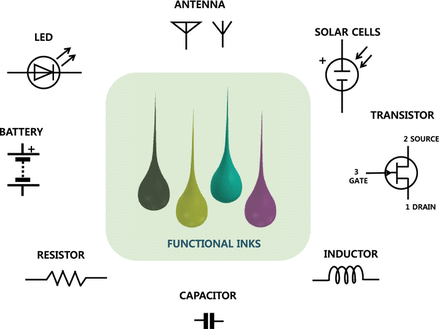
Printing technologies in an atmospheric environment offer the potential for low-cost and materials-efficient alternatives for manufacturing electronics and energy devices such as luminescent displays, thin-film transistors, sensors, thin-film photovoltaics, fuel cells, capacitors, and batteries. Significant progress has been made in the area of printable functional organic and inorganic materials including conductors, semiconductors, and dielectric and luminescent materials.
These new printable functional materials have and will continue to enable exciting advances in printed electronics and energy devices. Some examples are printed amorphous oxide semiconductors, organic conductors and semiconductors, inorganic semiconductor nanomaterials, silicon, chalcogenide semiconductors, ceramics, metals, intercalation compounds, and carbon-based materials.
A special focus issue of the ECS Journal of Solid State Science and Technology was created about the publication of state-of-the-art efforts that address a variety of approaches to printable functional materials and device. This focus issue, consisting of a total of 15 papers, includes both invited and contributed papers reflecting recent achievements in printable functional materials and devices.
The topics of these papers span several key ECS technical areas, including batteries, sensors, fuel cells, carbon nanostructures and devices, electronic and photonic devices, and display materials, devices, and processing. The overall collection of this focus issue covers an impressive scope from fundamental science and engineering of printing process, ink chemistry and ink conversion processes, printed devices, and characterizations to the future outlook for printable functional materials and devices.
The video below demonstrates Printed Metal Oxide Thin-Film Transistors by J. Gorecki, K. Eyerly, C.-H. Choi, and C.-H. Chang, School of Chemical, Biological and Environmental Engineering, Oregon State University.
This website uses cookies so that we can provide you with the best user experience possible. Cookie information is stored in your browser and performs functions such as recognising you when you return to our website and helping our team to understand which sections of the website you find most interesting and useful.

 Call for Papers
 Researchers have developed a new kind of semiconductor alloy capable of capturing the near-infrared light located on the edge of the visible light spectrum.