ECS Journal of Solid State Science and TechnologyIn a recently published ECS Journal of Solid State Science and Technology paper, ECS member Roger Loo and coauthors describe a new epitaxial growth technology and address the challenges of implementation. The open access article, “Epitaxial CVD Growth of Ultra-Thin Si Passivation Layers on Strained Ge Fin Structures,” was designated Editors’ Choice due to its significance and the importance of the technology described.

“The work combines carefully thought out and elegant experimental work, with appropriate simulation work that compliments the experiments,” said Jennifer Bardwell, ECS Journal of Solid State Science and Technology technical editor in the area of electronic materials and processing. “I am certain that it will be of great interest to many of our readers.”

We recently sat down with Loo to discuss the work and its impact on the field.

(more…)

Electrons
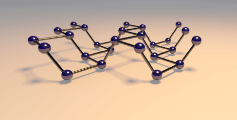
While tracking electrons moving through exotic materials, researchers have discovered intriguing properties not found in conventional, silicon-based semiconductors.

Unlike current silicon-based electronics, which shed most of the energy they consume as waste heat, the future is all about low-power computing. Known as spintronics, this technology relies on a quantum physical property of electrons—up or down spin—to process and store information, rather than moving them around with electricity as conventional computing does.

On the quest to making spintronic devices a reality, scientists at the University of Arizona are studying an exotic crop of materials known as transition metal dichalcogenides, or TMDs. TMDs have exciting properties lending themselves to new ways of processing and storing information and could provide the basis of future transistors and photovoltaics—and potentially even offer an avenue toward quantum computing.

(more…)

SemiconductorThe next generation of feature-filled and energy-efficient electronics will require computer chips just a few atoms thick. For all its positive attributes, trusty silicon can’t take us to these ultrathin extremes.

With two new semiconductors, however, it may be possible.

Electrical engineers have identified two semiconductors—hafnium diselenide and zirconium diselenide—that share or go beyond some of silicon’s desirable traits, starting with the fact that all three materials can “rust.”

“It’s a bit like rust, but a very desirable rust,” says Eric Pop, an associate professor of electrical engineering, who coauthored with postdoctoral scholar Michal Mleczko a paper on the research that appears in the journal Science Advances.

The new materials can also be shrunk to functional circuits just three atoms thick and they require less energy than silicon circuits. Although still experimental, the researchers say the materials could be a step toward the kinds of thinner, more energy-efficient chips demanded by devices of the future.

(more…)

Making the New Silicon

Shown here is the smallest laptop power adapter ever, made using GaN transistors.
Image: Cambridge Electronics

Recent discussions in the electronics industry have revolved around the future of technology in light of the perceived end of Moore’s law. But what if the iconic law doesn’t have to end? Researchers from MIT believe they have exactly what it takes to keep up with the constantly accelerating pace of Moore’s law.

More efficient materials

For the scientists, the trick is in the utilization of a material other than silicon in semiconductors for power electronics. With extremely high efficiency levels that could potentially reduce worldwide energy consumption, some believe that material could be gallium nitride (GaN).

MIT spin-out Cambridge Electronics Inc. (CEI) has recently produced a line of GaN transistors and power electronic circuits. The goal is to cut energy usage in data centers, electric cars, and consumer devices by 10 to 20 percent worldwide by 2025.

Semiconductors shaping society

Since its discovery in 1947, the transistor has helped make possible many wonders of modern life – including smartphones, solar cells, and even airplanes.

Over time, as predicted by Moore’s law, transistors became smaller and more efficient at an accelerated pace – opening doors to even more technological advancements.

(more…)

Building Better Electronic Devices

The development of the silicon chip forever changed the field of electronics and the world at large. From computers to cellphones to digital home appliances, the silicon chip has become an inextricable part of the structure of our society. However, as silicon begins to reach its limits many researchers are looking for new materials to continue the electronics revolution.

Fan Ren, Distinguished Professor at the University of Florida and Technical Editor of the ECS Journal of Solid State Science and Technology, has based his career in the field of electronics and semiconductor devices. From his time at Bell Labs through today, Ren has witnessed much change in the field.

Future of Electronics

Upon coming to the United States from Taiwan, Ren was hired by Bell Labs. This hub of innovation had a major impact on Ren and his work, and is where he first got his hands-on semiconductor research. During this time, silicon was the major player as far as electronic materials went. While electronics have transformed since that time, the materials used to create integrated circuits have essentially stayed the same.

People keep saying of other semiconductors, “This will be the material for the next generation of devices,” says Ren. “However, it hasn’t really changed. Silicon is still dominating.”

(more…)

Power Behind the Next Electronics Revolution

The semiconducting silicon chip brought about a wave of electronic transformation the propelled technology and forever changed the way society functions. We now live in a digital world, where almost everything we encounter on a daily basis is comprised of a mass of silicon integrated circuits (IC) and transistors. But with the materials used to develop and improve these devices being pushed to their limits, the question of the future of electronics arises.

The Beginnings

The move towards a digital age really took flight late in 1947 at Bell Labs when a little device known as the transistor was developed. After this development, Gordon Moore became a pioneering research in the field of electronics and coined Moore’s law in 1965, which dictated that transistor density would double every two years.

Just over 50 years after that prediction, Moore’s law is still holding true. However, researchers and engineers are beginning to hit a bit of a roadblock. Current circuit measurement are coming in a 2nm wide—equating to a size roughly between a red blood cell and a single strand of DNA. Because the integrated circuits are hitting their limit in size, it’s becoming much more difficult to continue the projected growth of Moore’s law.

The question then arises of how do we combat this problem; or do we move toward finding an alternative to silicon itself? What are the true limits of technology?

(more…)

New Material to Make Better Transistors

According to new research, black phosphorus may have the potential to outpace silicon.Image:

According to new research, black phosphorus may have the potential to outpace silicon.
Image: McGill University

We’re one step closer to atomic layer transistors due to recent research by a team of McGill University and Université de Montréal researchers. The new findings are the result of multidisciplinary work that yielded evidence that the material black phosphorus may make it possible to pack more transistors on a chip.

Researchers from McGill University joined with ECS’s Richard Martel in the Université de Montréal’s Department of Chemistry to examine if black phosphorus could tackle the prominent issue in the electronics field of designing energy-efficient transistors.

Similar to graphite, black phosphorus can be separate easily into single atomic layers to allow for thin transistors. When researchers are able to produce thinner transistors, they are also more efficient.

(more…)

Shortcut to Solar Cells

black-silicon

The newly developed black silicon has the potential to simplify the manufacturing of solar cells due to the ability of the material to more efficiently collect light.
Image: Barron Group

One of the roadblocks in developing a new, clean energy infrastructure lies in our ability to manufacture solar cells with ease and efficiency. Now, researchers from Rice University may have developed a way to simplify this process.

In Andrew Barron’s Rice University lab, he and postdoctoral student Yen-Tien Lu are developing black silicon by employing electrodes as catalysts.

The typical solar cell is made from silicon. By swapping that regular silicon for black silicon, solar cells gain a highly textured surface of nanoscale spikes that allows for a more efficient collection of light.

This from Rice University:

Barron said the metal layer used as a top electrode is usually applied last in solar cell manufacturing. The new method known as contact-assisted chemical etching applies the set of thin gold lines that serve as the electrode earlier in the process, which also eliminates the need to remove used catalyst particles.

(more…)

Silicon is the common material used in solar cells and computer chips, but gallium arsenide is an alternative material with many advantages. Image: YouTube/Stanford University

Silicon is the common material used in solar cells and computer chips, but gallium arsenide is an alternative material with many advantages.
Image: YouTube/Stanford University

When we think of chips and solar cells, we think of silicon. However, silicon isn’t the only chip-making material out there.

Researchers from Stanford University are turning their attention away from silicon and are looking toward gallium arsenide to make faster chips and more efficient solar cells.

Gallium arsenide is a semiconductor material with extraordinary properties. Electrons can travel six times faster in gallium arsenide than in silicon, allowing for faster operation of transistors. Unfortunately, cost effectiveness is not one of gallium arsenide’s alluring properties—which has caused researchers to opt for the much cheaper and less effective silicon material.

One single wafer of gallium arsenide could cost up to $5,000, whereas the same size wafer of silicon costs only $5.

(more…)

Paper-like Material to Boost Li-ion Batteries

The newly developed silicon nanofiber structure allow the battery to be cycled hundreds of times without significant degradation.Image: Nature Scientific Reports

The newly developed silicon nanofiber structure allows the battery to be cycled hundreds of times without significant degradation.
Image: Nature Scientific Reports

Electric cars and personal electronics may get the battery boost they need with this new development in lithium-ion batteries.

Researchers from the University of California, Riverside have created silicon nanofibers that are 100 times thinner than human hair, which will provide the potential to boost the amount of energy that can be delivered per unit weight of the batteries.

The research has been detailed in the paper “Towards Scalable Binderless Electrodes: Carbon Coated Silicon Nanofiber Paper via Mg Reduction of Electrospun SiO₂ Nanofibers.”

This from University of California, Riverside:

The nanofibers were produced using a technique known as electrospinning, whereby 20,000 to 40,000 volts are applied between a rotating drum and a nozzle, which emits a solution composed mainly of tetraethyl orthosilicate (TEOS), a chemical compound frequently used in the semiconductor industry. The nanofibers are then exposed to magnesium vapor to produce the sponge-like silicon fiber structure.

(more…)

  • Page 1 of 2
    • 1
    • 2