
Topic Close-up #6
Symposium G06: Materials and Processes for Semiconductor, 2.5 and 3D Chip Packaging, and Interconnection PCB 2
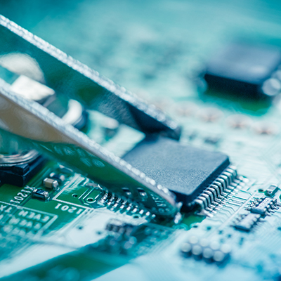
Symposium focus: This symposium focuses on issues pertinent to advances in semiconductor interconnects beyond the 20 nm technology node as well as novel materials and integration methods for 2.5D and 3D interconnects. Damascene interconnects using copper or cobalt, introduced at the 10-20 nm node, are expected to be used for the foreseeable future. The 2.5D or 3D concept replaces long 2D interconnects with shorter vertical interconnects, which have the potential to alleviate the interconnect delay. Since electrochemical processes are the ultimate solution to create smaller size and lower cost devices, both practical and fundamental aspects of electrochemical processes are of high interest. This symposium will bring researchers together to discuss various aspects of device design and architecture, novel materials, chemical formulation, packaging approaches, and nano-scale fabrication methodologies.
Invited speakers: More than 10 invited talks from industries and academia are planned, as well as many active discussions from contributed speakers.
For additional information on this topic close-up and more, check out the full call for papers with all the 236th ECS Meeting topics being held in Atlanta, GA on October 13-17, 2019.