Do you want to be forever externalized? Then look no further than this new quartz coin that can store the history of humankind for 14 billion years.

As if the previous breakthrough of quartz glass storage that yielded a self-life of 300 million years wasn’t enough, the new research take nanotechnology to a whole new level.

To understand exactly how long 14 million years is, check out these stats via Futurism:

  • Age of Earth: 4.534 billion years
  • Age of the Universe: 13.82 billion years

The research comes out of Southampton University, where the group has essentially developed a way to fit on just one sliver of nanostructured quartz 350TB of information.

This form Futurism:

The technique uses femtosecond laser pulses to write data in the 3D structure of quartz at the nanoscale. The pulses create three layers of nanostructred dots, each just microns above the other. The changes in the structure can be read by interrogating the sample with another pulse of light and recording the orientation of the waves after they’ve passed through.

Read the full article.

At the very least, this development in 5D storage will change the way we archive historical information.

New Semiconductor Material for Faster Electronics

The newly developed semiconductor material could eventually lead to electronic devices that are 100 percent faster.
Image: Dan Hixson/University of Utah College of Engineering

Thanks to a new development in semiconducting materials, our electronics may soon be faster all while consuming a lot less power.

The semiconductor is comprised of tin and oxygen and is only one atom thick, which allows electrical charges to move very quickly – much faster than comparable materials, such as silicon. This material also differs from conventional 3D materials, as it is 2D. The benefit of this material being 2D lies in the reduction of layers and thickness, thus allowing electronics to move faster.

This material has the ability to be applied to transistors, which are central to the majority of electronic devices.

This from the University of Utah:

While researchers in this field have recently discovered new types of 2D material such as graphene, molybdenun disulfide and borophene, they have been materials that only allow the movement of N-type, or negative, electrons. In order to create an electronic device, however, you need semiconductor material that allows the movement of both negative electrons and positive charges known as “holes.” The tin monoxide material discovered by Tiwari and his team is the first stable P-type 2D semiconductor material ever in existence.

(more…)

Graphene Simplifies Ice Removal

Graphene ice removal

Through a nanoribbon-infused epoxy, researchers were able to remove ice through Joule heating.
Image: Rice University

Graphene, better known as the wonder material, has seemingly limitless possibilities. From fuel cells to night-vision to hearing, there aren’t many areas that graphene hasn’t touched. Now, researchers from Rice University and transforming graphene for uses in air travel safety.

James Tour, past ECS lecturer and molecular electronics pioneer, has led a team in developing a thin coating of graphene nanoribbons to act as a real-time de-icer for aircrafts, wind turbines, and other surfaces exposed to winter weather.

(MORE: Read “High-Density Storage, 100 Times Less Energy“)

Through electrothermal heat, the graphene nanoribbons melted centimeter-thick ice on a static helicopter rotor blade in a -4° Fahrenheit environment.

This from Rice University:

The nanoribbons produced commercially by unzipping nanotubes, a process also invented at Rice, are highly conductive. Rather than trying to produce large sheets of expensive graphene, the lab determined years ago that nanoribbons in composites would interconnect and conduct electricity across the material with much lower loadings than traditionally needed.

Read the full article.

“Applying this composite to wings could save time and money at airports where the glycol-based chemicals now used to de-ice aircraft are also an environmental concern,” Tour said.

The coating may also protect aircrafts from lightning strikes and provide and extra layer of electromagnetic shielding.

New Device to Capture Bio-Data

An interdisciplinary team from multiple institutions in South Korea has recently developed a novel stretchable memory device that can be applied to the skin and used to monitor heart rate, which they believe outpaces current biosensor technology in this field.

With bio-data capturing devices on the rise in popular culture, researchers are working to increase efficiency and stability in these devices. The main problem with the current technologies is that the devices do not sit close enough to the skin. To combat this issues, the researchers have developed a new array that can be applied directly to the skin and can withstand stretching.

This from TechXplore:

The memory array is nonvolatile and made from fully multiplexed silicon and nanocrystal floating gates. The resulting device architecture built by the team is approximately the size of a human thumb and consists of two main parts, an array of ECG electrodes that are used for reading the heart rate, and the memory array—the two are connected together by a bit of electronics that also serve as amplifiers. The result is a patch-like device that is able to be stretched because the membrane material between each of the tiny squares circuits that make up both of the arrays, is flexible.

Read the full article.

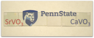
penn-state-materialA new material developed at Penn State could mean big things for everything from smartphones to solar cells.

For over 60 years, the main material used in transparent conductor display has been indium tin oxide. With over 90 percent of the display market utilizing this material, it has left very little room for competitor materials.

While indium tin oxide has provided solid efficiency levels at a decent price point for the past half decades, expenses have recently skyrocketed on this material.

Current electronic devices, such as smart phones and tables, are primarily priced according to display material costs. Displays and touch screen modules make up 40 percent of the cost to produce a device, greatly outpacing other essential pieces such as chips and processors. It hasn’t been until now that researchers have found a material that could potential replace indium tin oxide and potentially reduce device costs.

(more…)

World’s Most Expensive Material

The world’s most expensive material is being created in a lab and it’s going for $33,000 per 200 micrograms. To put that in perspective, that’s an astonishing $4.2 billion an ounce.

The novel material consists of molecular units called endohedral fullerenes, which are essentially a cage of carbon atoms containing nitrogen atoms.

Developers and scientists behind the material are focused on implementing the endohedral fullerenes into the development of a small, portable atomic clock. The atomic clock is the most accurate time-keeping system in the world and could assist in the accuracy of everything from a GPS to an automatic car.

“Imagine a minaturised atomic clock that you could carry around in your smartphone,” says Kriakos Porfyrakis, scientist working on the development of the material. “This is the next revolution for mobile.”

Aside from impacting cellphone technology, Porfyrakis expects the material to change transportation in a big way.

ICYMI: Learn about the early history of the Buckyball.

“There will be lots of applications for this technology,” says Lucius Cary, director of Oxford Technology SEIS fund. “The most obvious is in controlling autonomous vehicles. If two cars are coming towards each other on a country lane, knowing where they are to within 2m is not enough but to 1mm it is enough.”

Tiny Sensor Powered by Radio Waves

With smart technology on the rise, researchers are looking for ways to develop smaller sensors that can help building the landscape of the internet of things. However, this could potentially demand huge sums of power in an era where people are working hard to conserve energy. A research team from Eindhoven University of Technology may have found a solution to this problem with the development of their new extra-small, wireless sensors that are powered by radio waves that make up its wireless network.

With a router nearby, the tiny sensors can pull the necessary energy to give them functionality. The sensor is just 2 millimeters and can communicate temperatures.

This from Gizmodo:

Aboard the chip, a small antenna captures energy from the signals transmitted by the router. Once it’s charged, the sensor quickly switches on, measures the temperature, and then transmits a small signal for the router to detect. The frequency of the transmitted signal relates to the measured temperature.

Read the full article.

The researchers predict that the primary use for this sensor will be embedding the device within buildings to monitor conditions. Currently priced at 20 cents per sensor, researchers hope that with continued research, its potential could increase to detecting movement, light, and humidity.

The major issue right now lies in the fact that the sensor can only transmit its signal 2.5 centimeters. While the device is currently not practical, the team believes that its reach can grow to 16 feet with more research.

[Image: Eindhoven University of Technology]

Building a Biosensor from Bubblegum

What does Doublemint gum have to do with biomedical research? Apparently, a lot more than would be expected.

A combined research effort from the University of Manitoba and the Manitoba Children’s Hospital has recently created a stretchy, highly sensitive biosensor using chewed gum and carbon nanotubes.

After the gum in chewed for about 30 minutes, it is then cleaned with ethanol and laced with carbon nanotubes. The biosensor has the potential to monitor berating patterns and blood flow.

Even more impressive, the cost for the sensor come in under $3. Researchers believe the cheap, highly flexible biosensor could aid in a multitude of health care applications.

PS: Working in sensor science and technology? Make sure to check out our sensor symposia at the 229th ECS Meeting! Submit your abstract today!

Quantum Dots Make Infrared Light Visible

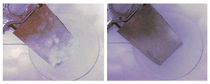
565db23d4c4abQuantum dots may be just the thing to take renewable energy technology to the next level.

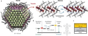
A team from MIT has recently developed a double film coating that has the ability to transform infrared light into visible light.

While that may not outwardly seem like a huge gain for the energy technology sector, the development has the potential to vastly improve efforts in renewable. Essentially, this research could help increase the amount of light a solar cell could capture. By capturing and using protons below their normal bandgap and thus converting the typically unused infrared light into use visible light, researchers could see efficiency levels of solar panels rise.

The researchers went about this development by placing two films on top of a plate of glass. The bottom film was comprised by using a type of quantum dot, while the top layer was made up of an organic molecule.

(more…)

Rusnanoprize Awarded to ECS Members

id41860Two ECS members were recently awarded the 2015 RUSNANOPRIZE Nanotechnology International Prize for their work in developing nanostructured carbon materials, which have facilitated the commercialization and wide-use of supercapacitors in energy storage, automotive, and many other industries. The organization honored Yury Gogotsi and Patrice Simon for their exemplary research in this field.

The RUSNANOPRIZE Nanotechnology International Prize, established in 2009, is presented annually to those working on nanotechnology projects that have substantial economic or social potential. The prize is aimed to promote successful commercialization of novel technology and strengthening collaboration in the field of nanotechnology.

Yury Gogotsi is a professor at Drexel University and director of the Anthony J. Drexel Nanotechnology Institute. Among his most notable accomplishments, Gogotsi was a member of a team that discovered a novel family of two-dimensional carbides and nitrides, which have helped open the door for exceptional energy storage devices. Additionally, Gogotsi’s hand in discovering and describing new forms of carbon and the development of a “green” supercapacitor built of environmentally friendly materials has advanced the field of energy technology.

Gogotsi is a Fellow of ECS and is currently the advisor of the Drexel ECS Student Chapter.

Patrice Simon is a professor at Paul Sabatier University. As a materials scientist and electrochemist, Simon has special interest in designing the next generation of batteries and supercapacitors. As the leader of the French Network on Electrochemical Energy Storage, Simon is making strides in developing next-gen technology through combining 17 labs and 15 companies in an effort to apply novel principals to issues in energy storage and technology. As an internationally recognized leader in the field of nanotechnology for energy storage, Simon’s work focuses on benefiting the entire energy storage industry.

Simon has been a member of ECS for 15 years.

ICYMI: Find other ECS researchers are doing in the world of nanocarbons.