
An interview with Isamu Akasaki
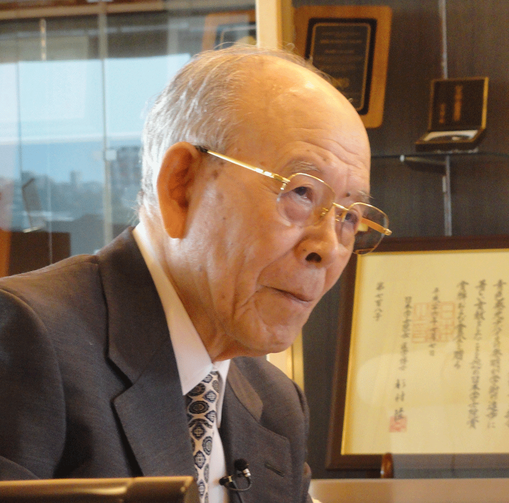 On June 8, 2016, Yue Kuo, an ECS fellow and vice president of The Electrochemical Society, traveled to the Akasaki Institute at Nagoya University in Japan to talk with Isamu Akasaki, a Nobel Prize winner and ECS life member.
Professor Akasaki is a materials scientist specializing in semiconductor science and technology. He is a pioneer of efficient blue light-emitting diodes which have enabled bright and energy-saving white light sources. He shares the 2014 Nobel Prize in Physics with Hiroshi Amano and Shuji Nakamura for this work. Prior to their groundbreaking work, scientists had produced LEDs that emitted red or yellow-green light, but not blue. Blue had been thought impossible or impractical to make. Blue LEDs became commercially available in 1994.
The new combination of blue, green, and red LEDs produces white light, and blue LEDs coated with YAG:Ce yellow phosphor appear white to the eye and can be developed for much less energy than that from incandescent and fluorescent lamps, which contain toxic mercury. Prof. Akasaki’s work helped lead to the development of blue semiconductor lasers, which proved useful for high-capacity optical-media devices such as Blu-ray disc players.
What follows is an edited transcript of the conversation between Yue Kuo and Isamu Akasaki, which they had in English.
Yue Kuo: Professor Akasaki, thank you for spending the time to talk with me. I represent ECS in congratulating you for your outstanding achievements in science. Hopefully, you can share your experiences
with our scientific community all over the world, and give special advice to our members and also to young researchers.
Isamu Akasaki: Thank you. Yes.
YK: Maybe you can start by talking about your background and growing up.
IA: I was born in Chiran in Kagoshima Prefecture. It’s the southern part of Kyushu Island. It’s a small town on the peninsula, but I grew up in the city of Kagoshima. I graduated from Kyoto University in 1952 and joined the Kobe Kogyo Corporation, now Fujitsu Limited, where I worked on fluorescent materials, screens, and vacuum tubes for TV.
YK: CRTs?
IA: Yes, CRTs. A powder was applied to the inner surface of the tubes, and the fluorescent screen emitted a high light when they were excited by the electron beam radiations. I have been working on luminescence (light emission without heat generation) ever since this first experience.
I noticed a considerable amount of light was absorbed by the powder. This made me wonder if it would be possible to make a brighter image by applying transparent single crystals rather than powders. We now call this epitaxial growth of light-emitting crystalline film, but it was nothing but a pipe-dream at that time.
It was then that the transistor first appeared, and they were mainly on a single crystal. And transistors were being investigated at the Kobe headquarters of the company. Being a semiconductor, germanium does not emit light. Still, single crystal rather than powders appealed to me.
In 1959, I moved to the newly created Department of Electronics at Nagoya University here, where I held the position of research associate, assistant professor, and then associate professor. Then, in 1964, I was invited to the newly established Matsushita Research Institute Tokyo, which was a new laboratory established by the late Konosuke Matsushita, the founder of Matsushita Electric, now Panasonic Company.
YK: So he had a vision?
IA: Right. And the purpose of this new institute was for researchers, and new, quite new, materials and new devices for future electronics. This is where I started to do the research exploring electronic materials and devices.
In 1968, I developed high quality gallium arsenide with the world’s highest electron mobility by vapor phase epitaxy. And in 1970, my group developed the brightest gallium phosphide red LED known at the time. In 1967, I began vapor phase epitaxial growth of aluminum nitride—not the gallium nitride, but aluminum nitride—and determined the angular frequencies of the longitudinal and the transverse optical-phonons by fitting the calculated reflectivity to the Reststrahlen band, which we found in the grown AlN crystal. It’s a material which I later used as a buffer material when we grew GaN on sapphire substrate in 1985. In the 1980s, I considered AlN, GaN, SiC, and ZnO as a buffer material to buffer strain between GaN and sapphire, and we chose AlN at the beginning because I had been familiar with AlN since 1967.
I had an insight during the early stage of gallium nitride based semiconductor research, into the great potential of the blue light emitters, and to pioneer a new field founded on the unique properties of nitride semiconductors, namely the toughness, the wider direct energy gaps, the higher thermal conductivity, and also nontoxicity.That is a short history of my work before I grew gallium nitride single-crystal.
(Ed. Note: In 1999, Dr. Akasaki was awarded the ECS Solid State Science and Technology Award, now called the Gordon E. Moore Medal for Outstanding Achievement in Solid State Science and Technology. He had with him during this interview the original notes he used to make his acceptance speech. Below is an excerpt from what he read to Dr. Kuo.)
IA: It is a great honor and a real pleasure for me to be awarded the ECS Solid State Science and Technology Award. … I started research work on semiconductor in 1959. That was a time when I worked on epitaxial vapor growth of germanium. … I am deeply moved that the research on wide-band gallium nitride and the related materials are currently one of the most “hot” research areas. It took just a quarter century, since 1974, when I first grew the gallium nitride single crystal film by molecular beam epitaxy. … Because of the help of many coresearchers and students, I am indebted to say that without their support, it would not have been possible.
I really owe my accomplishment to my collaborators at Matsushita Research Institute Tokyo, Y.Koide and H.Amano, and the many co-researchers at Nagoya University. I’m very thankful to my seniors, colleagues, and family members who have enlightened and supported me…. Finally, but not least, I’d like to wish The Electrochemical Society continued prosperity for many years to come. Thank you very much!
YK: That’s great. If I can have this copy, I’ll send it to ECS for their records. Thank you. Would you say the first blue LED was presented at an ECS meeting?
IA: Yes. That was an oral presentation, and a very short abstract.
YK: That’s very important. I don’t know if you’re aware, for example in semiconductor, another very important paper we talk about is Gordon Moore’s, and Moore’s law. Similar to your occasion, Moore’s law was first articulated at an ECS section meeting.
IA: Really?
YK: Yes. ECS is very glad to have the most important papers published in ECS journals. This is very important historical information. Would you talk about your philosophy? You have done research for so many years, you must have developed your own personal view.
IA: Philosophy?
YK: Yes.
IA: No pain, no gain. And as Thomas Edison said, “Genius is one percent inspiration and 99 perspiration.” (Ed. Note: Thomas Edison was an ECS member for 28 years, having joined the Society in 1903.) I say this to younger people, experience is the best teacher. That is, sometimes there is no royal road to learning.
YK: That’s very useful advice. I’m sure when you started working with gallium nitride, probably a lot of people resisted it by saying, “Why do you do this?” Was it very tough to persuade people?
IA: That (gallium nitride) is a tough material, so that is very important, most important. And most people had given up on gallium nitride research, or shifted to zinc selenide. But I worried about the instability of zinc selenide.On the other hand, the gallium nitride is very tough, has a wider energy gap which means that it can be used with UV emitters, and a very high electron saturation mobility. This means that it is very promising for high-speed/high-powered devices. So I didn’t think to do research on zinc selenides.
YK: Never?
IA: Never.
YK: But when you started, even aluminum nitride, at that time must have been a novel idea.
IA: Yes. I grew aluminum nitride crystals in 1967, and I first studied its optical properties and then made blue phosphor. But I wasn’t satisfied with the photoluminescence or cathodoluminescence. I wanted to make electroluminescence, so I thought to make aluminum gallium nitride mixed crystals, but at that time it was too difficult. Of course, I made aluminum gallium nitride, but actually the data showed a mixture of AlN and GaN, not an AlGaN alloy. Not so the other times that I didn’t use MOVPE (metalorganic vapour phase epitaxy).
YK: There was no MOCVD (metalorganic chemical vapour deposition)?
IA: Yes. And MOVPE was proposed by H.M.Manasevit, et al., and this had succeeded in many variety of compounds, except gallium nitride. Manasevit’s group published only one paper on the growth of
nitrides by this method in 1971, but never employed the method for the growth of nitride semiconductors thereafter.
(Ed. Note: The paper mentioned here was published by ECS. See H. M. Manasevit, F. M. Erdmann, and W. I. Simpson, “The Use of Metalorganics in the Preparation of Semiconductor Materials: IV. The Nitrides of Aluminum and Gallium,” J. Electrochem. Soc., 118, 1864 (1971).)
Crystal quality is greatly affected by the growth method and condition. GaN can be grown by HVPE (hydride vapor phase epitaxy) proposed by P. Maruska, et.al., by MBE, or by MOVPE (also called
OMVPE or MOCVD). I compared these methods.
In the case of HVPE, crystal quality was degraded by appreciable reverse reactions, and the growth rate was too fast to fabricate device structure with thin layers of nanometers. MBE was prone to nitrogen deficiency and the growth rate was so slow at that time. On the other hand, MOVPE seemed to be the method that was more suitable for the growth of GaN, because this method has advantages as follows:
1. This method simply has no reverse reactions.
2. All the source materials are gasses, so that all the important parameters, such as growth rate, AlGaN, GaInN alloy compositions, and also impurity doping could be readily controlled by the flow rate of the source gasses.
Note that the growth rate, alloy composition control, and impurity doping are very important to produce high-performance LEDs and laser diodes.
Thus, I decided to adopt MOVPE as the optimal growth method for GaN and its alloys in 1979 at Matsushita Research Institute Tokyo.
The second decision was a substrate. I chose sapphire as the substrate as before, because it was chemically stable even under harsh MOVPE growth condition (1000°C in NH3 atmosphere and is relatively similar to GaN in terms of crystal symmetry). Actually the fact that today’s GaN crystals and LEDs are mostly grown on sapphire by MOVPE proves that these decisions were not wrong. MOVPE has more fractions in the other ways. The same thing with gallium aluminum nitride.
YK: I see. So this is one of the most important methods?
IA: Yes I think so. In 1979, I decided to adopt MOVPE.
YK: Yes, that’s very important.
IA: The first time we reported growth of gallium nitride by MOVPE was in 1984.
YK: From your experience, do you remember if there was a moment when you felt, “Wow, this must be it?” Sometimes we get good work, research, and people may not feel it’s important but we say, “I know
this is important.” Eventually someday, people recognize it.
IA: It’s, yes. This is my personal, I’m not sure if this English is correct or not.
(Ed. Note: Dr. Akasaki showed Dr. Kuo a sentence of Kanji, which is a Japanese version of Chinese characters on an old philosophy that means “My way is penetrated by a single thread.”)
YK: Yes, I understand. That’s important. I think this was probably talked about first by Confucius. That’s basic physics.
Let us summarize our conversation. What would be a very good summarization of your research or your advice? And do you think this sentence (Yue Kuo points to the philosophic sentence Prof. Akasaki showed before) would be good for the young people to stick to?
No pain, no gain, I think everyone can understand it. It is very important. I really appreciate you spending the time to talk with me and the members of ECS.
IA: Please give them my best regards.
(Read and download at no cost, Isamu Akasaki’s research published by ECS.)
This article was originally published in Interface. Read the original article.