201st Meeting - Philadelphia, PA
May 12-17, 2002
PROGRAM INFORMATION
J1 - International Symposium on Plasma Processing XIV
Dielectric Science and Technology/Electronics/High Temperature Materials
Monday, May 13, 2002
Salon L, Level 5
Plasma Enhanced CVD
Co-Chairs: G.S. Mathad and S. Panda
| Time | Abs# | Title |
|---|
| 10:00 | 399 |
Process and Material Properties of PECVD Boron-Doped Amorphous Silicon Film - H. Nominanda and Y. Kuo (Texas A '&' M University) |
| 10:20 | 400 |
Properties of Boron Doped Amorphous Silicon Films Obtained with a Low Frequency Plasma - A.
Heredia-J, A. Torres-J, A. Jaramillo-N, F.J. De la Hidalga-W, C. Zuniga-I, and A. Munguia
(Instituto Nacional de Astrofisica) |
| 10:40 | 401 |
Characteristics of Low Temperature Polysilicon Thin Film Deposited Using SiF4 and D2 Gas Mixture in PECVD System - S.C.
Bae, G.H. Rue, and S.Y. Choi (Kyungpook National University) |
| 11:00 | 402 |
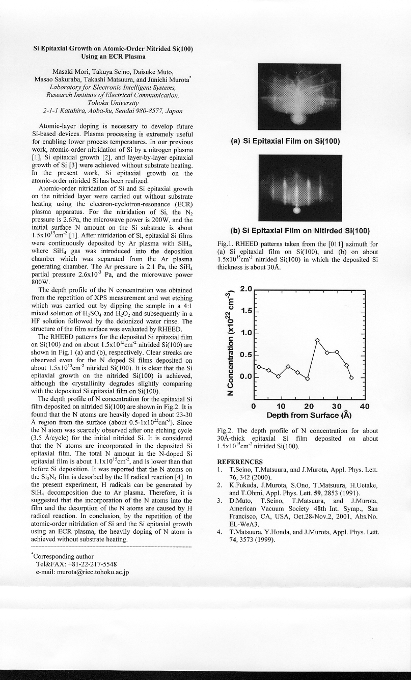
Si Epitaxial Growth on Atomic-Order Nitrided Si(100) Using an ECR Plasma - J.
Murota, M. Mori, T. Seino, D. Muto, M. Sakuraba, and T. Matsuura (Tohoku University) |
| 11:20 | 403 |
Prediction of Deposition Rates in Plasma-Enhanced Atomic Layer Deposition - V. Prasad (Rensselaer Polytechnic Institute), S.C. Foster,
M.K. Gobbert (University of Maryland), and T.S. Cale (Rensselaer Polytechnic Institute) |
| 11:40 | 404 |
High-Density Plasma Deposited Silicon Nitride Films for Coating InGaAs High-Power Lasers -
R.E. Sah, F. Rinner, R. Kiefer, M. Mikulla, and G. Weimann (Fraunhofer-Institut fur Angewandte
Festkorperphysik) |
Plasma Etching I: Modeling Mechanisms
Co-Chairs: G.Oehrlein and Y. Kuo
| Time | Abs# | Title |
|---|
| 2:00 | 405 |
High Productivity 300mm HDP-CVD for Next-Generation Gap Fill Processes - P.
Krishnaraj, N. Dubey, and B. Geoffrion (Applied Materials, Inc.) |
| 2:20 | 406 |
Plasma Hydrogenation of a Buried Trap Layer in Silicon: Formation of a Platelet Layer - A. Usenko (Silicon Wafer Technologies, Inc.), W. Carr, and B. Chen (New Jersey Institute of Technology) |
| 2:40 | 407 |
The Evolution of Plasma Etching in Integrated Circuit Manufacturing - J. Coburn (University of California at Berkeley) |
| 3:20 | |
Twenty-Minute Intermission - |
| 3:40 | 408 |
Integrated Modeling Investigation of Plasma Dielectric Etching Processes - D. Zhang, S.
Rauf, T. Sparks, and P. Ventzek (Motorola) |
| 4:00 | 409 |
Beam Study of Plasma-surface Kinetics and Simulation of Feature Profile Evolution in Cl_2 and HBr Etching of Polysilicon - W. Jin, S. Vitale, and H. Sawin (MIT) |
| 4:20 | 410 |
Ion Energy Dependence of the Etch Selectivity of Low-k Polymer to Si3N4 Etch Stopper by N2 and NH3 Plasma Beam Irradiation - Y. Yamaoka, K.
Kurihara, K. Karahashi, M. Sekine, and M. Nakamura (Association of Super-Advanced Electronics Technologies) |
| 4:40 | 411 |
Surface Treatment of SiC Using NF3/O2 Plasma - T. Kai, W. Shimizu, K. Tanaka
(Doshisha University), T. Abe, M. Inaba, Z. Ogumi (Kyoto University), T. Tojo (Toyo Tanso
Co.,Ltd), and A. Tasaka (Doshisha University) |
Tuesday, May 14, 2002
Plasma Etching II: Equipment
Co-Chairs: J. Coburn and K. Mautz
Plasma Etching III: Gate Dielectrics and Silicon
Co-Chairs: R.E. Sah and V. Bakshi
| Time | Abs# | Title |
|---|
| 2:00 | 416 |
Differential Surface Charging of the Dielectric During Plasma Etching and Surface Charge Leakage Kinetic -
M.K. Abatchev, B.J. Howard, D.S. Becker, R.L. Stocks, and J. Chapman (Micron Technology, Inc.) |
| 2:20 | 417 |
Thickness Scaling of Gate Dielectric on Plasma Charging Damage in MOS Devices - K.-S.
Chang-Liao and P.-J. Tzeng (National Tsing Hua University) |
| 2:40 | 418 |
Gate Oxide Integrity and Microloading Characterization of 300mm Process Tools - K. Mautz (Motorola, Inc.) |
| 3:00 | 419 |
Measurement of Device Charging Damage in a Dielectric Etch 300mm Chamber with a Bias Voltage Diagnostic Cathode - M.
Kutney, S. Ma, K. Horioka, R. Lindley, S. Kats, T. Kropewnicki, K. Doan, D. Lane, and H. Shan (Applied Materials, Inc., Dielectric Etch Division) |
| 3:20 | |
Twenty-Minute Intermission - |
| 3:40 | 420 |
Etching of High K Gate Dielectric and Gate Metal Electrode Candidates -
S.K. Han, I. Kim, G.P. Heuss, H. Zhong, V. Misra, and C.M. Osburn (North Carolina State University) |
| 4:00 | 421 |
Etching of High Aspect Ratio Trenches - S. Panda (IBM Microelectronics), S.
Mathad, and R. Ranade (Infineon Technologies Corp.) |
| 4:20 | 422 |
Inverse Loading Effects in Reactive Ion Etching of Silicon - S. Jensen and O. Hansen (Technical University of Denmark) |
| 4:40 | 423 |
Plasma Etched Silicon Stampers for Plastic Biotechnology Applications - D. Weston, W.
Dauksher, D. Rhine, T. Smekal (Motorola Labs), S. Rauf, P. Strout, and P. Ventzek (Motorola Digital) |
| 7:30 | |
Panel Discussion - |
Wednesday, May 15, 2002
Plasma Etching IV: Silicon Dioxide
Co-Chairs: M.D. Allendorf and R.E. Sah
| Time | Abs# | Title |
|---|
| 9:00 | 424 |
Current Issues in Pattern Transfer into Dielectric Films by High-Resolution Plasma Etching Techniques - G.
Oehrlein, X. Li, X. Hua, L. Ling, X. Wang, and M. Fukasawa (University of Maryland) |
| 9:40 | 425 |
Radical Control in a Hole to Break an Etch-Stop Barrier for High Selective HARC Etching - N.
Negishi, K. Yokogawa (Hitachi Ltd.), T. Yoshida (Hitachi High-Technologies Corporation), and M. Izawa (Hitachi Ltd.) |
| 10:00 | 426 |
SiO2 Etching Characteristics of Perfluoro-2-butene(l-C4F8) and Hexafluoropropene(l-C3F6) - C.-H. Shin (Association of Super-Advanced Electronics Technologies), C.-J. Kang (Samsung Electronics Co., LTD.), A.
Egami, and N. Moritaka (Association of Super-Advanced Electronics Technologies) |
| 10:20 | 427 |
Etching and Deposition : The Effect on Profiles and Etching Yield Curves for Oxide Etching - O. Kwon, W. Jin, and H. Sawin (MIT) |
| 10:40 | |
Thirty-Minute Intermission - |
Plasma Etching V: Dual Damascene, Low-k
Co-Chairs: M. Yang and G.S. Mathad
| Time | Abs# | Title |
|---|
| 2:00 | 428 |
Plasma Etching of Silicon Nitride with High Selectivity over Silicon Oxide and Silicon in Fluorine Containing Plasmas - C.
Reyes-Betanzo, S. Moshkalyov (Center for Semiconductor Components), M. Cotta (IFGW), M. Pavanello (Center for Semiconductor Components), C. Ramos
(IFGW), and J. Swart (Center for Semiconductor Components) |
| 2:20 | 429 |
A Novel Approach to Reduce Micro-trenching and Via faceting in the Via-First, No Middle Stop Layer Dual Damascene Trench Etch - Y. Kim, K. Doan, and H. Shan (Applied Materials) |
| 2:40 | 430 |
Patterning 180 nm Copper-Oxide Dual Damascene Baseline with 193nm Resists - V. Bakshi and G. Smith (International
SEMATECH) |
| 3:00 | 431 |
Mechanism Producing Bowed Profiles in the Etching of Low-k Organic Films - S.
Sekiyama, K. Nakamura, and H. Yanazawa (Association of Super-Advanced Electronics Technologies) |
| 3:20 | |
Twenty-Minute Intermission - |
| 3:40 | 432 |
Analysis of Etched Low-k Organic Material Surfaces - K. Nakamura, S.
Sekiyama, and H. Yanazawa (Association of Super-Advanced Electronins Technologies) |
| 4:00 | 433 |
HBr Plasma Based Copper Etch Process - S. Lee and Y. Kuo (Texas A '&' M University) |
| 4:20 | 434 |
Intellectual Property Creation from Semiconductor Process and Equipment Development - K. Mautz (Motorola, Inc.) |
| 4:40 | 435 |
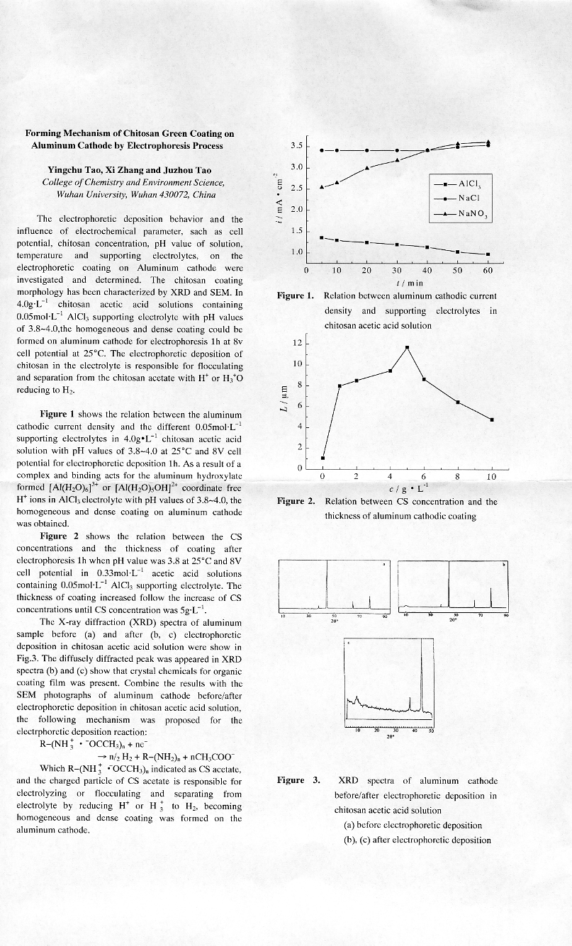
Forming Mechanism of Chitosan Green Coating on Aluminum Cathode by Electrophoresis Process - Y. Tao, X. Zhang, J. Tao, and J. Fu
(Wuha University) |
|