201st Meeting - Philadelphia, PA
May 12-17, 2002
PROGRAM INFORMATION
N1 - Ninth International Symposium On Silicon Materials Science and Technology
Electronics
Monday, May 13, 2002
Salon F, Level 5
Plenary Session
Co-Chairs: H.R. Huff and L. Fabry
Plenary Session
Co-Chairs: L. Fabry and S. Kishino
Plenary Session
Co-Chairs: S. Kishino and H.R. Huff
Tuesday, May 14, 2002
Silicon Materials 300 MM
Co-Chairs: W. Von Ammon and T. Shigematsu
Silicon Materials 300 MM
Co-Chairs: T. Shigematsu and W. Von Ammon
| Time | Abs# | Title |
|---|
| 9:50 | 564 |
Growth of 300 mm Silicon Single Crystals in a 24i+/- Hot Zone - H.
Tu, X. Dai, Z. Wu, G. Zhang, J. Wang, F. Fang, Q. Zhou, and Q. Xiao (National Engineering Research Center for Semiconductor Materials) |
| 10:10 | 565 |
Study on Geometry, Surface Damage and Rapid Thermal Annealing of 300 mm As-cut Silicon Wafers - G. Zhang, B. Liu, J.
Zhao, W. Chen, J. Wang, Q. Zhou, and H. Tu (National Engineering Research Center for Semiconductor Materials) |
| 10:30 | 566 |
Argon-Annealed 300mm Wafer Complementing pp-Epitaxial Layers - T. Muller, W. Siebert, R.
Wahlich, P. Krottenthaler, A. Ikari, K. Mebmann, R. Holzl, and W. von Ammon (Wacker Siltronic AG) |
Silicon Materials Generic Issues
Co-Chairs: W. Von Ammon and T. Shigematsu
| Time | Abs# | Title |
|---|
| 2:00 | 567 |
Thermophysical Properties of Intrinsic Point Defects in Crystalline Silicon - T. Sinno (University of Pennsylvania) |
| 2:30 | 568 |
Impact of Silcon Bulk Defects on Deep Submicron Design-Rule DRAM Services - E. Dorneberger
(Wacker Siltonic AG), D. Temmler (Infineon Technologies), and W. von Ammon (Wacker Siltonic AG) |
| 2:50 | 569 |
Fractional Contribution in Si Self-Diffusion: Dopant Concentration and Temperature Dependence on Si Self-Diffusion Mechanism - Y. Nakabayashi,
H.I. Osman, K. Toyonaga, K. Yokota, S. Matsumoto (Keio University), J. Murota (Tohoku University), K. Wada (Massachusetts Inst. of Technology), and T. Abe
(ShinEtsu Handootai) |
| 3:10 | 570 |
Effect of Vacancy Double Acceptor Level in Si Self-Diffusion Under Heavy Doping Condition -
H.I. Osman, Y. Nakabayashi, T. Sakaguchi, K. Toyonaga (Keio University), J. Murota (Tohoku University), K. Wada (Massachusetts Inst. of Technology), T. Abe
(ShinEtsu Handootai), and S. Matsumoto (Keio University) |
| 3:30 | 571 |
Wafers with Low LPD and Reduced Haze Prepared by Short Annealing Process -
J.L. Vasat, A.D. Stefanescu, T. Torack (MEMC Electronic Materials, Inc.), and R. Orizio
(MEMC Electronic Materials, Spa.) |
| 3:50 | |
Ten-Minute Intermission - |
Silicon Materials Generic Issues
Co-Chairs: T. Shigematsu and W. Von Ammon
| Time | Abs# | Title |
|---|
| 4:00 | 572 |
Oxidation-Induced Stacking Faults in Nitrogen Doped Czochralski Silicon - D. Yang, J.
Chu, X. Ma, L. Li, and D. Que (Zhejiang University) |
| 4:20 | 573 |
Impact of Nitrogen Doping in Silcon onto Gate Oxide Integrity - A. Huber, M. Kasper, J.
Grabmeier, U. Lambert, W.V. Ammon, and R. Pech (Wacker Siltronic AG) |
| 4:40 | 574 |
Atomic Layer Doping of N in Si Epitaxial Growth on Si (100) and its Thermal Stability - J.
Murota, Y.C. Jeong, M. Sakuraba, and T. Matsuura (Tohoku University) |
| 5:00 | 575 |
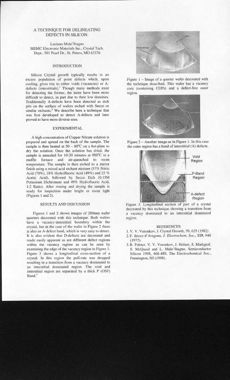
A Technique for Delineating Defects in Silicon - L. Mule'Stagno
(MEMC Electronic Materials Inc.) |
| 5:20 | 576 |
Growth Technology for 200 mm Antimony Heavily Doped Silicon Single Crystals - Q.
Zhou, F. Qin, J. Zhou, F. Fang, J. Wang, and H. Tu (National Engineering Research Center for Semiconductor Materials) |
| 5:40 | 577 |
Silicon Epitaxy and Particle Dynamics: A Theoretical and Experimental Study - S. Kommu
(MEMC Electronic Materials, Inc.) |
Process Modeling
Co-Chairs: H. Richter and P. Mertens
Wednesday, May 15, 2002
Alternative Materials and IC Processing Technologies
Co-Chairs: H. Iwai and W. Maszara
| Time | Abs# | Title |
|---|
| 8:30 | 581 |
SOI Technology: The Future Will Not Scale Down - S. Cristoloveanu
(IMEP, ENSERG) |
| 9:00 | 582 |
SiGeC Device Applications - H.J. Osten
(IHP) |
| 9:30 | |
Ten-Minute Intermission - |
| 9:40 | 583 |
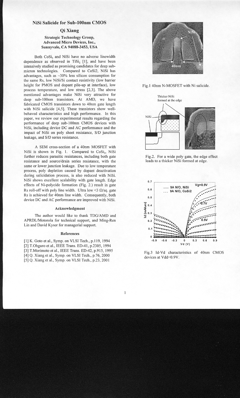
NiSi Salicide for Sub-100nm CMOS - Q. Xiang (Advanced Micro Devices, Inc.) |
| 10:10 | 584 |
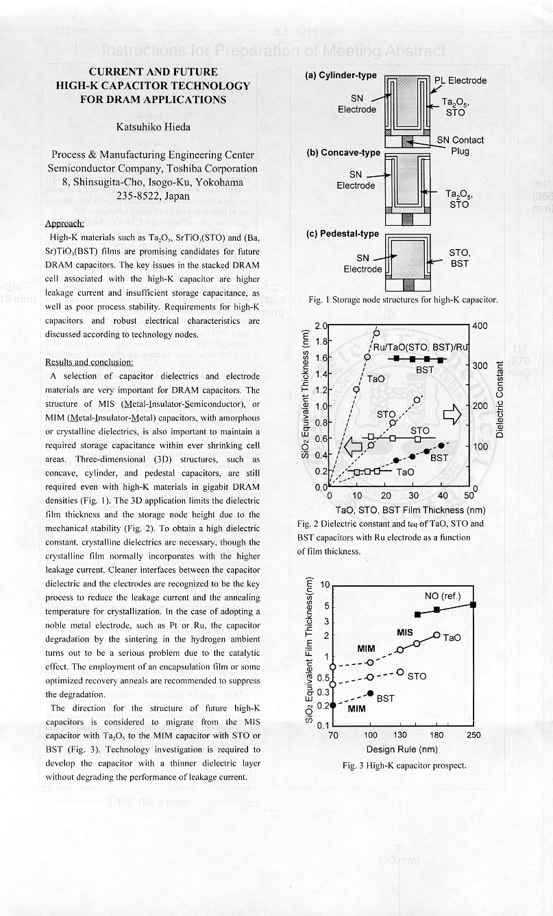
Current and Future High-K Capacitor Technology for DRAM Applications - K. Hieda (Toshiba Corporation) |
| 10:40 | 585 |
Rare Earth Metal Oxides for High-K Gate Insulator - S. Ohmi, S. Akama, A. Kikuchi, I. Kashigwagi, C. Ohshima, J. Taguchi, H. Yamamoto, K. Sato, M. Takeda, H. Ishiwara, and H. Iwai (Tokyo Inst. of Technology) |
Alternative Materials and IC Processing Technologies
Co-Chairs: W. Maszara and H. Iwai
| Time | Abs# | Title |
|---|
| 2:00 | 586 |
Electronic Structure of Non-crystalline High-k Transition-metal and Rare Earth Oxides and Their Silicate and Aluminate Alloys - Y. Zhang, G. Lucovsky, B. Rayner, G. Appel, and J. Whitten (NC State University) |
| 2:20 | 587 |
Interpretation of Non-linear Chemical Shifts in XAP/AES Features in Non-crystalline Zirconium Silicate Alloys: (ZrO2)x(SiO2)1-x - B. Rayner, D. Kang, and G. Lucovsky (North Carolina State University) |
| 2:40 | 588 |
Interface Reactions During Oxygen Plasma Assisted Chemical Vapor Deposition of Yttrium Oxide on Silicon - D. Niu, R. Ashcraft (North Carolina State University), S. Stemmer (Rice University), and G. Parsons (North Carolina State University) |
| 3:00 | 589 |
Study of Diffusivity and Electrical Properties of Zr and Hf in Silicon - O. Vyvenko, R. Sachdeva, A. Istratov, R. Armitage, E. Weber (University of California), P.N.K.(S. Deenapanray, C. Jagadish (Australian National University), Y. Gao (Applied Microanalysis Labs), and H. Huff (International Sematech) |
| 3:20 | |
Ten-Minute Intermission - |
Process Modeling
Co-Chairs: P. Mertens and H. Richter
| Time | Abs# | Title |
|---|
| 3:30 | 590 |
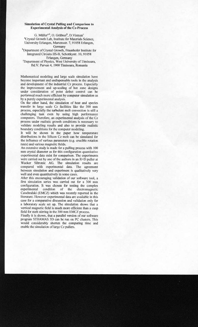
Simulation of Crystal Pulling and Comparison to Experimental Analysis Cz-Process - G. Muller (University Erlangen), O. Grabner (Fraunhofer Inst. for Integrated Circuits), and D. Vizman (West University of Timisoara) |
| 4:00 | 591 |
Grown in Microdefect Distribution in Doped Silicon Crystals - G. Borionetti, D. Gambaro, M. Porrini, and V. Voronkov (MEMC Electronic Materials) |
| 4:20 | 592 |
Calculation of Size Distribution of Void Defect in Czochralski Silicon - M. Akastsuka, M. Okui, S. Umeno, and K. Sueoka (Sumimoto Metal Industries Ltd.) |
| 4:40 | 593 |
Modelling of Crystal Originated Particles and their Impact on Gate Oxide Integrity - T. Bearda, P. Mertens (Interuniversity Micro-Electronics Center), P. Woerlee, H. Wallinga (University of Twente), R. Schmolke (Wacker Siltronic AG), and M. Heyns (Interuniversity Micro-Electronics Center) |
| 5:00 | 594 |
Computer Simulation for Morphology , Size, and Density of Oxide Precipitates in Czochraiski Silicon - K. Sueoka, M. Akatsuka, M. Okui, and H. Katahama (Sumimoto Metal Industries, Ltd.) |
| 5:20 | 595 |
Simulation of the Point Detect Diffusion and Growth Condition for Defect-free Silicon Crystal - K. Nakamura, T. Saishoji, and J. Tomioka (Komatsu Electronic Metals Co., Ltd.) |
| 5:40 | 596 |
Modeling of SiGe Epitaxial Growth in a Wide Range of Growth Conditions - A. Segal, A. Sid'ko, S. Karpov (Soft Impact Ltd), and Y. Makarov (STR, Inc) |
Thursday, May 16, 2002
Process Modeling
Co-Chairs: H. Richter and P. Mertens
| Time | Abs# | Title |
|---|
| 8:00 | 597 |
Unified Theory of Thermal Silicon Oxide Growth - M. Uematsu, H. Kageshima, and K. Shiraishi (NTT Basic Research Labs) |
| 8:30 | 598 |
Characterization of the Mechanical Stress Induced During silicidation in Sub-0.25UM Mos Technologies - A. Steegen (IBM Microelectronics) |
| 9:00 | 599 |
Gettering Efficiencies and Their Depence on Material Parameters and Thermal Processes: How Can This Be Modeled? - R. Hoelzl, M. Blietz, L. Fabry, and R. Schmolke (Wacker Siltronic AG) |
| 9:30 | |
Ten-Minute Intermission - |
| 9:40 | 600 |
Modeling of Competitive Gettering Between Devices and Gettering Sites - A. Istratov (University of California, Berkeley), W. Huber (Sumitomo Sitix Silicon), and E. Weber (University of California, Berkeley) |
| 10:00 | 601 |
Determination of Minimum Oxygen Precipitate Growth Conditions for Gettering of Copper and Nickel - M. Seacrist, M. Stinson, J. Libbert, R. Standley, and J. Binns (MEMC Electronic Materials, Inc.) |
| 10:20 | 602 |
Effective Intrinsic Gettering for 200mm and 300mm P/P- Wafers in a Low Thermal Budget 0.13um Advanced CMOS Logic Process - M. Binns, S. Bertolini (MEMC Electronic Materials Inc.,), R. Wise, D. Myers, and T. McKenna (Texas Instruments Incorporated) |
| 10:40 | |
Ten-Minute Intermission - |
Process Modeling
Co-Chairs: P. Mertens and H. Richter
| Time | Abs# | Title |
|---|
| 10:50 | 603 |
Bulk Micro Defects of p/p- Epitaxial Silicon Wafers with Nitrogen Doped Substrates and Their Gettering Behavior - R. Schmolke, M. Blietz, R. Holzl, D. Menzel (Wacker Siltonic AG), and H. Bender (IMEC) |
| 11:10 | 604 |
First Principles Calculations for Nitrogen-Vacancy Related Defects in N-CZ Si - A. Karoui, F. Sahtout Karoui, G.A. Rozgonyi (North Carolina State University), M. M. Hourai, and K. K. Sueoka (Sumitomo Metal Industries, Ltd.) |
| 11:30 | 605 |
The Control of Boron Autodoping During Device Processing for P/P+ Epi-Wafers With No Back-Surface Oxide Seal - M. Binns, S. Kommu, M. Seacrist, R. Standley (MEMC Electronic Materials, Inc), R. Wise, D. Myers, D. Tisserand, and D. Doyle (Texas Instruments Incorporated) |
| 11:50 | 606 |
Impact of State-of-the-art Cz Substrates on the Current-Voltage Characteristics of Shallow p-n Junctions - A. Poyai, E. Simoen, C. Claeys (IMEC), A. Huber, D. Graf (Wacker Siltronic AG), and E. Gaubas (Vilnius University) |
Process Integration
Co-Chairs: P. Tobin and S. Deleonibus
| Time | Abs# | Title |
|---|
| 2:00 | 607 |
Invention of Stacked Capacitor DRAM Cell - M. Koyanagi (Tohoku University) |
| 2:30 | 608 |
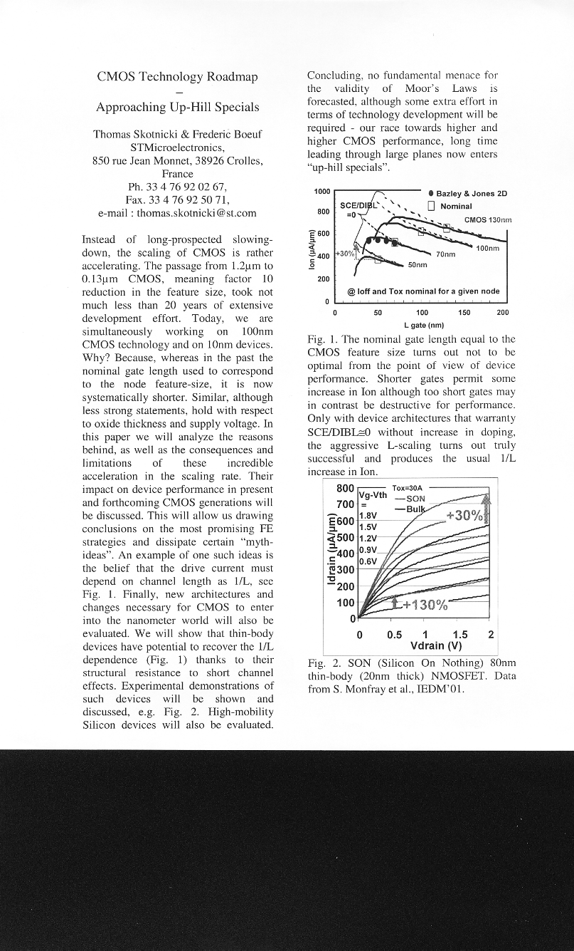
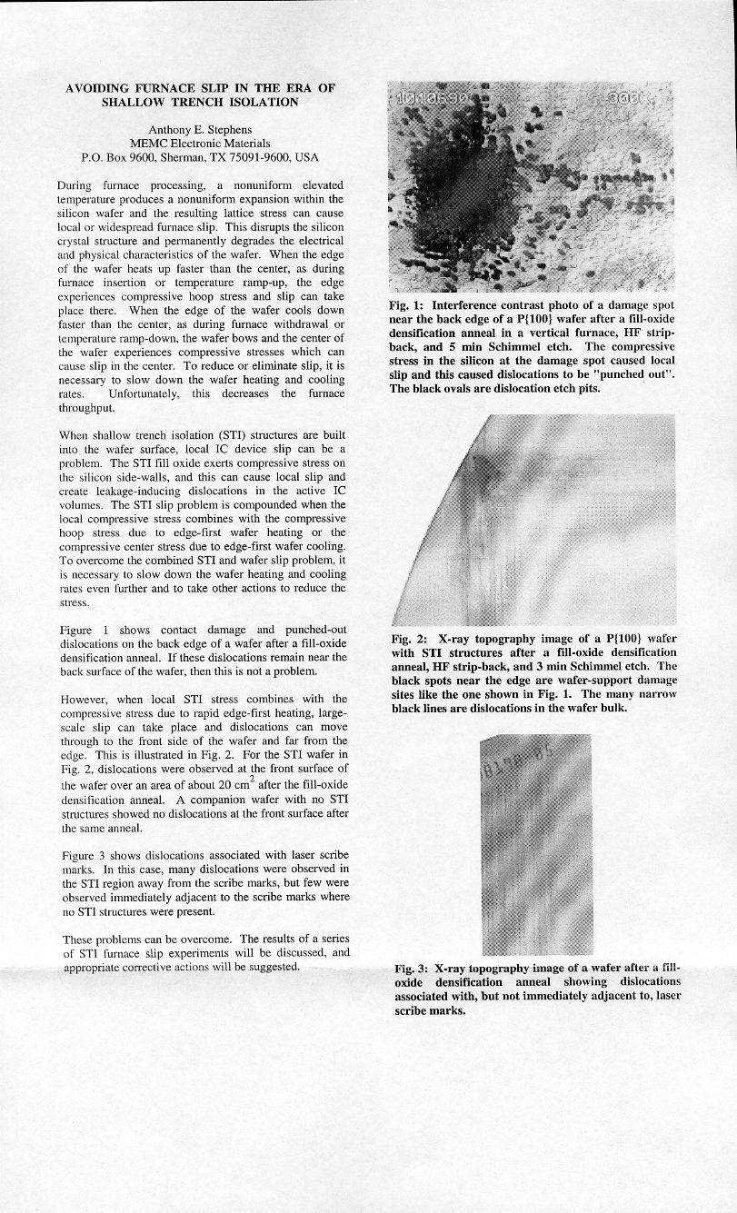
CMOS Technology Roadmap: Approaching Up-Hill Specials - T. Stotnicki and F. Bouef (STMicroelectronics) |
| 3:00 | 609 |
The High K Challenges in CMOS - E. Young (International SEMATECH) |
| 3:30 | 610 |
Integration Issues of Polysilicon with High k Dielectrics Deposited by Atomic Layer Chemical Vapor Deposition - W. Tsai, J. Chen (International Sematech), R. Carter, E. Cartier (IMEC), J. Kluth (International Sematech), O. Richard (IMEC), M. Claes (ASM International), Y.M. Lin (International Sematech), Y. Manabe, H. Nohira, T. Conard, M. Caymax (IMEC), E. Young (International Sematech), W. Vandervorst, S. Degendt, M. Heyns (IMEC), J.W. Maes (ASM International), C. Rittersma, and F. Roozeboom (Philips Research) |
| 3:50 | |
Ten-Minute Intermission - |
Process Integration
Co-Chairs: S. Deleonibus and P. Tobin
| Time | Abs# | Title |
|---|
| 4:00 | 611 |
A New Junction Technology Based on Selective CVD of Sige for CMOS Technology Nodes Beyond 30 NM - M. Ozturk, N. Pesovic, J. Liu, H. Mo, I. Kang, and S. Gannavaram (North Carolina State University) |
| 4:30 | 612 |
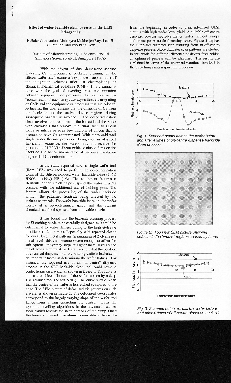
Avoiding Furnace Slip in the Era of Shallow Trench Insulation - A.E. Stephens (MEMC Electronic Materials) |
| 4:50 | 613 |
Effective Intrinsic Gettering of Copper During a Sub-quarter Micron CMOS Process - K.-M. Bae, J.-R. Kim, Y.-K. Hong (MEMC Korea Co. Ltd.), S.-I. So, S.-C. Lee, S.-S. Kim, S.-W. Ha, C.-G. Koh, S.-H. Pyi (Hynix Semiconductor), and D.-M. Lee (MEMC Electronic Materials, Inc.) |
| 5:10 | 614 |
Damascene Metal Gate for 70 NM Cmos Process - B. Guilaumot (STM Microelectronics), F. Ducroquet (UMR), G. Guegan, C. Renard, B. Previtali (CEA), M. Rivoire, M.E. Nier (STM Microelectronics), S. Tedesco, T. Fargeot, H. Achard, and S. Deleonibus (CEA) |
| 5:30 | 615 |
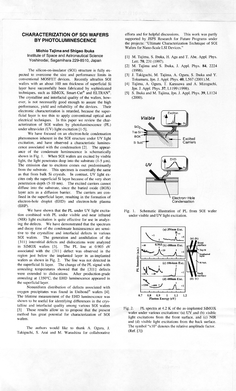
Effect of Wafer Backside Clean Process on the ULSI Lithography - N. Balasubramanian, R. Moitreyee-Mukherjee, P. Lau. H. G., and F.P. Dow (Instite of Microelectronics) |
Friday, May 17, 2002
Integrated Metrology and Diagnostics
Co-Chairs: A. Diebold and H. Koyama
Integrated Metrology and Diagnostics
Co-Chairs: H. Koyama and A. Diebold
| Time | Abs# | Title |
|---|
| 10:20 | 621 |
Measurement of Nitrogen Concentration in CZ Silicon - N. Inoue, K. Shingu, and K. Matsumoto (Japan Electronics & Information Technology Association) |
| 10:50 | 622 |
Experimental Method to Determine an Acceptable Concentration of Iron Impurity in Hot Zone Structural Components - H. Sreedharamurthy, M. Seacrist, J. Holder, and M. Banan (MEMC Electronic Materials, Inc.) |
| 11:10 | 623 |
Effect of Oxide Thickness on Dielectric Breakdown Induced by Surface COP - K. Yamabe, Y. Shimada, M. Piao, T. Yamazaki, T. Otsuki, R. Takeda, Y. Ohta, S. Jimbo, and M. Watanabe (GOI Task Force SOI Wafer Committee) |
| 11:30 | 624 |
Microroughness Analysis of Silicon Wafers Using Ultraviolet Raman Microscopy - J. Wang, H. Tu, B. Liu, Q. Zhou, and W. Zhu (National Engineering Research Center for Semiconductor Materials) |
| 11:50 | 625 |
The Behaviour of Oxygen in Oxygenated N-Type High-Resistivity Float-Zone Silicon - E. Simoen, C. Claeys (IMEC), R. Job, A. Ulyashin, W. Fahrner (University Hagen), G. Tonelli (INFN), O. Degryse, and P. Clauws (University of Ghent) |
Ultimate Silicon and End-of-Roadmap Devices
Co-Chairs: S. Hillenius and S. Ishihara
| Time | Abs# | Title |
|---|
| 1:30 | 626 |
50 nm Vertical Replacement-Gate (VRG) nMOSFETs with ALD HfO_2 Gate Dielectrics - J. Hergenrother, T. Nigam, G. Wilk, F. Klemens, D. Monroe, T. Sorsch, B. Busch, M. Green (Agere Systems), D. Muller, P. Voyles, J. Grazul (Bell Laboratories, Lucent Technologies), E.J. Shero, M.E. Givens, C. Pomarede, M. Mazanec, and C. Werkhoven (ASM America) |
| 2:00 | 627 |
Electrochemical Properties of Nanometer-Scale Mosfets - H. Kawaura and T. Sakamoto (NEC Corporation) |
| 2:30 | 628 |
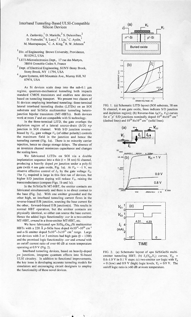
Interband Tunneling-Based ULSI-Compatible Silicon Devices - A. Zaslavsky (Brown University), D. Mariolle, S. Deleonibus, D. Fraboulet (LETI), S. Luryi (SUNY at Stony Brook), J. Liu, C. Aydin (Brown University), M. Mastrapasqua, R.W. Johnson, and C.A. King (Agere Systems) |
| 2:50 | |
Ten-Minute Intermission - |
Ultimate Silicon and End-of-Roadmap Devices
Co-Chairs: S. Ishihara and S. Hillenius
| Time | Abs# | Title |
|---|
| 3:00 | 629 |
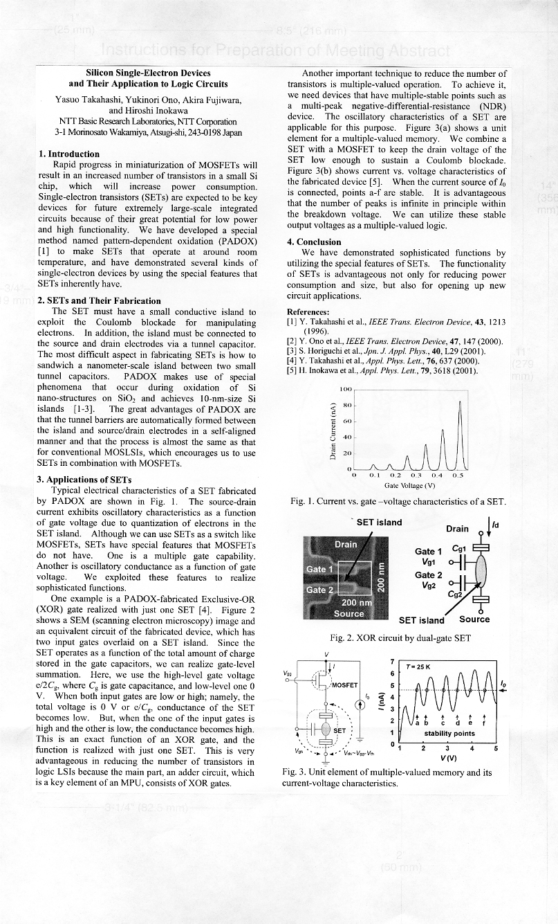
Silicon Single-Electron Devices and Their Application to Logic Circuits - Y. Takahashi, Y. Ono, A. Fujiwara, and H. Inokawa (NTT Corporation) |
| 3:30 | 630 |
Single-electron and Nanoscopic Device Evolution - F. Kreupl (Infineon Technologies AG) |
| 4:00 | 631 |
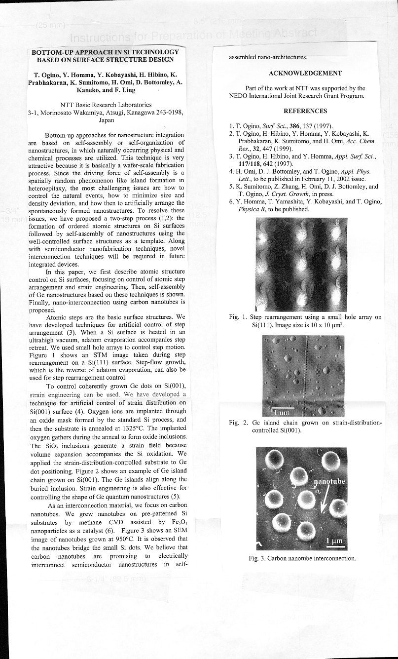
Bottoms-up Approach in Si Technology Based on Surface Structure Design - T. Ogino, Y. Homma, Y. Kobayashi, H. Hibino, K. Prabhakaran, K. Sumitomo, H. Omi, D. Bottomley, A. Kaneko, and F. Ling (NTT Basic Research Labs) |
|