
 Topic Close-up #2
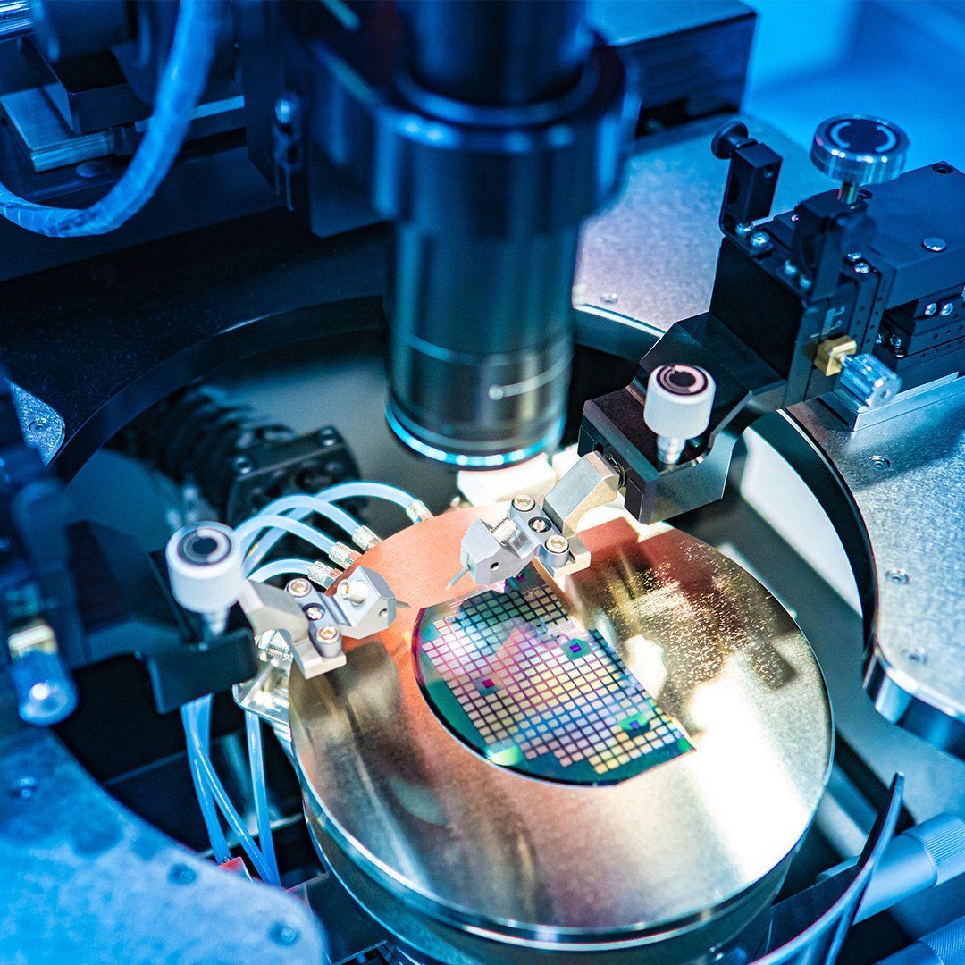
Symposium: H02—Semiconductor Wafer Bonding: Science, Technology and Applications 17
Extended abstract deadline:
April 21, 2023
Submit today!
Symposium focus: Semiconductor wafer bonding continues to evolve as a crucial technology extending new integration schemes in diverse areas as three-dimensional (3D) device integration using copper/oxide bonding, high quality silicon-on-insulator (SOI) materials for microelectronics device applications. Up to now, semiconductor bonding is performed mainly at the wafer scale level with wafer-to-wafer bonding (W2W). It is noteworthy that during recent years, die-to-wafer (D2W) bonding is starting to become increasingly mature. Originally devoted to photonic applications allowing the III/V semiconductor world to work on silicon CMOS platforms, 3D D2W hybrid bonding is now entering into industrial fabs.
For more information, please consult the Call for Papers.