Scientists from Tohoku University in Japan have developed a new type of energy-efficient flat light source based on carbon nanotubes with very low power consumptions of around 0.1 Watt for every hour's operation -- about a hundred times lower than that of an LED.Credit: N. Shimoi/Tohoku University

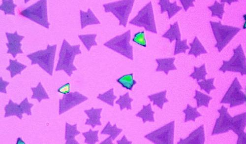
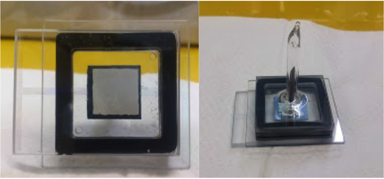
Scientists have developed a new type of energy-efficient flat light source with a power consumption about a hundred times lower than that of an LED.
Credit: N. Shimoi/Tohoku University

Scientists all around the globe are constantly looking for a way to create the even-better-bulb of tomorrow. In order to do this, researchers are looking toward carbon electronics.

This from the American Institute of Physics:

Electronics based on carbon, especially carbon nanotubes (CNTs), are emerging as successors to silicon for making semiconductor materials, and they may enable a new generation of brighter, low-power, low-cost lighting devices that could challenge the dominance of light-emitting diodes (LEDs) in the future and help meet society’s ever-escalating demand for greener bulbs.

Read the full article here.

With this in mind, scientists from Tohoku University have developed a new type of energy-efficient flat light source with a very low power consumption that comes in around 0.1 Watt for every hour of operation. This is about one hundred times lower than that of an LED.

(more…)

The researchers discovered that two flat semiconductor materials can be connected edge-to-edge with crystalline perfection.Credit: University of Washington

The researchers discovered that two flat semiconductor materials can be connected edge-to-edge with crystalline perfection.
Credit: University of Washington

Current member of ECS, Xiaodong Xu, has made a huge contribution to the field of electrochemical science with the creation of atomically seamless, thinnest-possible semiconductor junctions.

Xu, along with the scientists at the University of Washington, believe their semiconductor – coming in at only three atoms thick – is the most slender possible, a new class of nanoscale materials.

This from the University of Washington:

The University of Washington researchers have demonstrated that two of these single-layer semiconductor materials can be connected in an atomically seamless fashion known as a heterojunction. This result could be the basis for next-generation flexible and transparent computing, better light-emitting diodes, or LEDs, and solar technologies.

Read the full article here.

“Our experimental demonstration of such junctions between two-dimensional materials should enable new kinds of transistors, LEDs, nanolasers, and solar cells to be developed for highly integrated electronic and optical circuits within a single atomic plane,” Xu said.

The research was published online this week in Nature Materials.

Find more research from Xu published in our Digital Library.