
Edgar’s new patented process will allow for the building of better semiconductors.
Source: Kansas State University
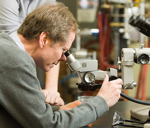
The Electrochemical Society’s Jim Edgar has developed a new process to build better semiconductors, which will vastly improve the efficiency of electronic devices and help propel the semiconductor industry.
Edgar, a Kansas State university distinguished professor of chemical engineering and an active member of ECS since 1981, has just received a patent for his “Off-axis silicon carbide substrates” process, which is a way to build a better semiconductor. This new process could mean big things for the electronics and semiconductor manufacturing industries.
“It’s like a stacked cake separated by layers of icing,” Edgar said. “When the layers of semiconductors don’t match up very well, it introduces defects. Any time there is a defect, it degrades the efficiency of the device.”
Edgar’s process will minimize these potential defects.
“We have applied this process to other systems,” Edgar said. “We are working on verifying that it is not just these specific materials we started with, but that it can be applied to a lot of different materials.”
[Source: Kansas State University]Make sure to join Edgar and other brilliant scientific minds by becoming a member of ECS today!