

Roger Loo
The Electrochemical Society hosted “Epitaxial Si/SiGe Multilayers for novel logic and memory devices” a live webinar by Roger Loo (imec) on May 6, 2026. A live question and answer session followed. Answers to some of the questions not addressed during the broadcast follow.
Replay webinarQ&A
How do you avoid TSVs (thru silicon vias)?
This presentation did not cover the post epi device fabrication steps. For this question, we kindly refer the audience to the work published by Anabela Veloso et al 2024 ECS Trans. 113 13, https://iopscience.iop.org/article/10.1149/11302.0013ecst
Are you using mocvd or mbe for these epi layers?
Epi layers have been grown on 300 mm wafers using the CVD tool from ASM (Intrepid® ES™)
CFET edge dislocations were resolved with low temperature, but this was not the case for the 3D-DRAM superlattice. 3D-DRAM superlattice still had edge dislocations and embedded defects with low temperature processing. Is this because of the thickness difference between the two applications?
Correct, between both stacks, there is a strong difference in the total SiGe thickness (3D DRAM with 30-120 bilayers –> SiGe thickness: 300 – 1200 nm compared to CFET: ~54 nm SiGe20% + 18 nm SiGe38%)
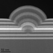
Are the defects on the top of the stacked layers linked to defects that form during epitaxy from high order silicon?
Correct, see this example of a cross-section (showing CFET stack, grown with a non-optimized processed based on higher order precursors)
What is the impetus for shifting from 100 to 110 wafers? Is there a cost or other benefit since the interfaces aren’t as sharp with 110?
(110) substrate orientation is considered for p-type MOS devices as it allows a higher hole mobility.
How is Ge diffusion into Si layers prevented here under annealing and operational conditions?
During epitaxial growth, when switching from SiGe to Si, Ge segregation is prevented by maintaining a Cl passivation of the growing surface.
After epi, Ge diffusion from SiGe into the Si channels is prevented by reducing the thermal budget during post-epi processing, see e.g. H. Mertens VLSI 2016, https://ieeexplore.ieee.org/document/7573416
Using a Si-SiGe channel can increase current, but what about leakage current and SS?
The SiGe is a sacrificial layer. It is selectively removed from the stack and replaced by the gate dielectric.
Learn more about upcoming ECS Webinars and review previous webinar recordings.
Interested in presenting in the ECS Webinar Series? Email your presentation title and abstract to education@electrochem.org for consideration.