
 Ya-Hsiang Tai, Chih-Chung Tu, Jia-Wei Fan, Yu-Sian Lin, Wang-Wei Ko, and Hsueh-Shih Chen present a compelling study of lead sulfide (PbS) quantum dot (QD)–based phototransistors designed for short-wave infrared (SWIR) thermal sensing. Published on February 19, 2026, this work provides a thoughtful comparison between 940 nm and 1600 nm PbS QD devices within a gap-type metal–semiconductor–metal (MSM) architecture.
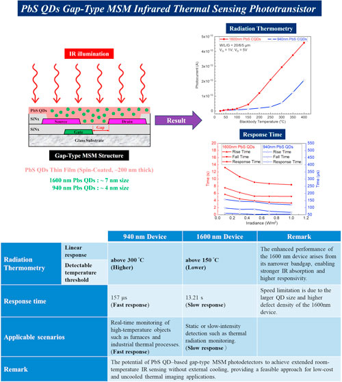
Tunable bandgap engineering influences device performance
A powerful demonstration of how tunable bandgap engineering can meaningfully influence device performance is at the heart of this ECS Journal of Solid State Science and Technology article The 1600 nm PbS QD device, benefiting from its narrower bandgap and stronger IR absorption, achieved a lower detectable temperature threshold and a linear photocurrent–temperature response above 150 °C. In contrast, the 940 nm device required temperatures exceeding 300 °C but offered a dramatically faster response time 157 μs compared to 13.21 s for the 1600 nm device.
This nuanced performance comparison highlights an important design insight: while the 1600 nm device is well suited for static or slowly varying thermal radiation, the 940 nm configuration excels in real-time monitoring of high-temperature objects. Together, these findings underscore the versatility of PbS QD–based thin-film phototransistors and their potential to enable low-cost, uncooled infrared sensing and thermal imaging technologies.
Device-level insights and broader implications
For researchers working in solid state devices, optoelectronics, infrared sensing, and quantum dot materials, this article provides both practical device-level insights and broader implications for scalable thermal detection solutions.We encourage the community to read the full article and explore how this innovative approach to PbS quantum dot engineering may inform your own research and applications in next-generation IR sensing technologies. Be sure to read this article today!
(Click to enlarge)