Graphene
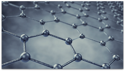
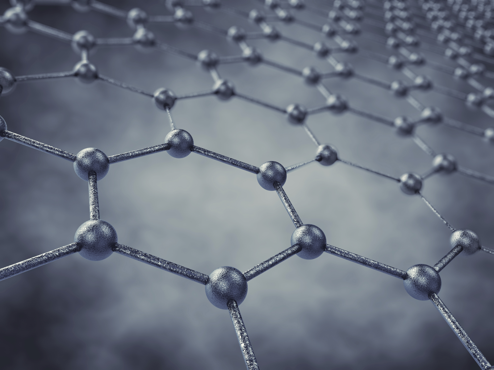
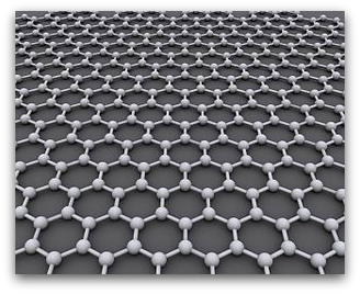
Graphene could offer a new way to cool tiny chips in phones, computers, and other gadgets.

“You can fit graphene, a very thin, two-dimensional material that can be miniaturized, to cool a hot spot that creates heating problems in your chip,” says Eva Y. Andrei, a physics professor at Rutgers University. “This solution doesn’t have moving parts and it’s quite efficient for cooling.”

As electronics get smaller and more powerful, there’s an increasing need to for chip-cooling solutions. Researcher show in a paper published in the Proceedings of the National Academy of Sciences that using graphene combined with a boron nitride crystal substrate creates a very efficient cooling mechanism.

“We’ve achieved a power factor that is about two times higher than in previous thermoelectric coolers,” says Andrei.

The power factor refers to the effectiveness of active cooling. That’s when an electrical current carries heat away, as shown in this study, while passive cooling is when heat diffuses naturally.

(more…)

Tagged

By: Mike Williams, Rice University

Graphene

Rice University researchers have modeled a nanoscale sandwich, the first in what they hope will become a molecular deli for materials scientists.

Their recipe puts two slices of atom-thick graphene around nanoclusters of magnesium oxide that give the super-strong, conductive material expanded optoelectronic properties.

Rice materials scientist Rouzbeh Shahsavari and his colleagues built computer simulations of the compound and found it would offer features suitable for sensitive molecular sensing, catalysis and bio-imaging. Their work could help researchers design a range of customizable hybrids of two- and three-dimensional structures with encapsulated molecules, Shahsavari said.

The research appears this month in the Royal Society of Chemistry journal Nanoscale.

The scientists were inspired by experiments elsewhere in which various molecules were encapsulated using van der Waals forces to draw components together. The Rice-led study was the first to take a theoretical approach to defining the electronic and optical properties of one of those “made” samples, two-dimensional magnesium oxide in bilayer graphene, Shahsavari said.

“We knew if there was an experiment already performed, we would have a great reference point that would make it easier to verify our computations, thus allowing more reliable expansion of our computational results to identify performance trends beyond the reach of experiments,” Shahsavari said.

(more…)

By: Mike Williams, Rice University

GrapheneA new type of conductive graphene foam is incredibly tough and can be formed into just about any shape and size.

A chunk of the foam, which is reinforced by carbon nanotubes, can support more than 3,000 times its own weight and easily bounce back to its original height.

The Rice University lab of chemist James Tour tested this new “rebar graphene” as a highly porous, conductive electrode in lithium ion capacitors and found it to be mechanically and chemically stable. The results appear in the journal ACS Applied Materials and Interfaces.

Carbon in the form of atom-thin graphene is among the strongest materials known and is highly conductive; multiwalled carbon nanotubes are widely used as conductive reinforcements in metals, polymers and carbon matrix composites. The Tour lab had already used nanotubes to reinforce two-dimensional sheets of graphene. Extending the concept to macroscale materials made sense, says Tour, a professor of computer science and of materials science and nanoengineering.

“We developed graphene foam, but it wasn’t tough enough for the kind of applications we had in mind, so using carbon nanotubes to reinforce it was a natural next step,” Tour adds.

(more…)

Nano-chimney to Cool Circuits

Overheating has emerged as a primary concern in the development of new electronic devices. A new study from Rice University looks to provide a solution to that, offering a strategy to vent heat away from nano-electronics through cone-like chimneys.

By putting these “chimneys” between the graphene and nanotube, the researchers effectively eliminate a barrier that typically blocks heat from escaping.

This from Rice University:

Researchers at Rice University discovered through computer simulations that removing atoms here and there from the two-dimensional graphene base would force a cone to form between the graphene and the nanotube. The geometric properties of the graphene-to-cone and cone-to-nanotube transitions require the same total number of heptagons, but they are more sparsely spaced and leave a clear path of hexagons available for heat to race up the chimney.

(more…)

Silly putty isn’t just for kids anymore.

Researchers in Ireland combined the classic kid’s toy with a special form of carbon to create a new material that has potential applications in medical devices such as heart monitors.


About 70 years ago, scientists came up with the recipe for silly putty as a substitute for rubber. The resulting formula yielded strange properties, but not many applications. However, by taking the strange silly putty formula and mixing it with graphene, the new mixture showed remarkable electrical, bouncy, liquid-like properties.

InSeNewly developed semiconductor materials are showing promising potential for the future of super-fast electronics.

A new study out of the University of Manchester details a new material called Indium Selenide (InSe). Like graphene, InSe if just a few atoms thick, but it differs from the “wonder material” in a few critical ways. While graphene has been hailed for its electronic properties, researchers state that it does not have an energy gap – making graphene behave more like a metal than a semiconductor.

Similarly, InSe can be nearly as thin as graphene while exhibiting electronic properties higher than that of silicon. Most importantly, InSe has a large energy gap, which could open the door to super-fast, next-gen electronic devices.

(more…)

GrapheneResearchers are shedding new light on cell biology with the development of a graphene sensor to monitor changes in the mitochondria.

The one-atom-thin layer of carbon sensor is giving researchers a new outlook into the process known as programmed cell death in mitochondria. The mitochondrion, which is found in most cells, has been known as the powerhouse of the cell due to its ability to metabolize and create energy for cells. However, the new researcher out of University of California, Irving shows that that convention wisdom on how cells create energy is only half right.

This from UC Irving:

[Peter] Burke and his colleagues tethered about 10,000 purified mitochondria, separated from their cells, to a graphene sensor via antibodies capable of recognizing a protein in their outer membranes. The graphene’s qualities allowed it to function as a dual-mode sensor; its exceptional electrical sensitivity let researchers gauge fluctuations in the acidity levels surrounding the mitochondria, while its optical transparency enabled the use of fluorescent dyes for the staining and visualization of voltage across the inner mitochondrial membranes.

(more…)

GrapheneOver the past few years, researchers have been exploring graphene’s amazing properties and vast potential applications. Now, a team from Iowa State University is looking to take those properties enabled by graphene and applied them to sensors and other technologies.

Many scientists have had a hard time moving graphene from the lab to the marketplace, but the research team from Iowa State University saw potential in using inkjet printers to create multi-layer graphene circuits and electrodes for the production of flexible, wearable electronics.

“Could we make graphene at scales large enough for glucose sensors?” ECS member and Iowa State University postdoctoral researcher, Suprem Das, wanted to know.

(MORE: Read more of Das’ work in the ECS Digital Library.)

The problem with the printing process is that the graphene would then have to be treated to improve its electrical conductivity, which could degrade the flexibility. Instead of using high temperatures and chemical to do this treatment, Das and other members of the team opted to use lasers.

(more…)

Researchers from Washington University in St. Louis have found a way to make dirty water drinkable with a light, affordable biofoam.

The newly developed bi-layered biofoam is made up of a bottom layer of bacteria-produced cellulose, which acts as a sponge and soaks up the dirty water. It then pushes that water to the top layer, which is comprised of graphene oxide. The graphene oxide then works to evaporate the filth, resulting in an end product of clean water.

“We hope that for countries where there is ample sunlight, such as India, you’ll be able to take some dirty water, evaporate it using our material, and collect fresh water,” says Srikanth Singamaneni, co-author of the study. “The beauty is that the nanoscale cellulose fiber network produced by bacteria has excellent ability to move the water from the bulk to the evaporative surface while minimizing the heat coming down, and the entire thing is produced in one shot.”

(more…)

Researchers around the world have been talking about the potential of “wonder material” graphene since it first entered the field of materials science. However, for all its promising theoretical potential and applications, we’ve yet to see the material make its way to the market. Now, after an announcement by Chinese-based Guangzhous OED Technologies, graphene may make its first appearance in the marketplace within the next year.

The company just announced that they have developed what they are claiming is the “world’s first graphene electronic paper.” The e-paper, which is a display device that mimics the appearance of ordinary ink on paper, is expected to be taken to further heights with this development.

This from Phys:

The group at OED claims to have developed a graphene material that is suitable for use in making e-paper. Doing so, they also claim, allows for creating screens that are more bendable and that are also brighter because they will be able to display light with more intensity. They also suggest that because the end product will be carbon based, it should be cheaper to manufacture than current e-paper products which are based on metal indium.

(more…)

  • Page 2 of 6