ECS Connections to 2014 Physics Nobel Prize

The 2014 Nobel Prize in Physics has been awarded to Shuji Nakamura, a professor at the University of California

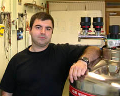
Shuji Nakamura, the recipient of the 2014 Nobel Prize in Physics and former ECS Plenary speaker, is awarded for his invention of efficient blue light-emitting diodes.
Credit: Randall Lamb

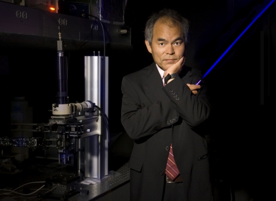
The 2014 Nobel Prize in Physics has been awarded to Shuji Nakamura, professor of materials and of electrical and computer engineering at the University of California and 2010 ECS Plenary speaker.

The prize is for the invention of efficient blue light-emitting diodes, which has enabled bright and energy-saving white light sources, and is shared with ECS member Isamu Akasaki of Meijo University and Nagoya University, Japan; and Hiroshi Amano of Nagoya University.

In his plenary talk at the 218th ECS Meeting in Las Vegas, Nevada, Nakamura described the current status of III-nitride based light emitting diodes (LEDs) and laser diodes. Nitride-based white LEDs have been used for many application such as LCD TV backlight, lighting for inside/outside applications and others.

According to the Royal Swedish Academy of Sciences, when Nakamura, Akasaki and Amono “produced bright blue light beams from their semiconductors in the early 1990s, they triggered a fundamental transformation of lighting technology. Red and green diodes had been around for a long time, but without blue light, white lamps could not be created. Despite considerable efforts, both in the scientific community and in industry, the blue LED had remained a challenge for three decades.”

The LED lamp “holds great promise for increasing the quality of life for over 1.5 billion people around the world who lack access to electricity grids,” the academy continued.

Here’s a list of articles in the ECS Digital Library written by the 2014 Physics Nobel Prize Winners. You can look at them for free:

Hiroshi Amano and Isamu Akasaki

Widegap Column-III Nitride Semiconductors for UV/Blue Light Emitting Devices

Growth and Luminescence Properties of Mg-Doped GaN Prepared by MOVPE

Isamu Akasaki

Epitaxial Growth and Properties of AIxGal.xN by MOVPE

Etching Characteristics and Light Figures of the {111} Surfaces of GaAs

Shuji Nakamura

Piezoelectric Field in Semi-Polar InGaN/GaN Quantum Wells

Read more about Shuji Nakamura’s plenary talk.

Read more about 2014 Nobel Prize winners for Physics.

What’s Graphene?

Kostya Novoselov

Published over 60 peer-refereed research papers (mainly as the principal/corresponding author) including Nature and Science articles and more than 15 papers in Nature Materials, Nature Physics, Nature Nanotechnology, Reviews of Modern Physics, Physical Review Letters, PNAS.

We’ve been having lots of talks around the home office about how people don’t realize the impact of electrochemistry and solid state science have on their world.

Being new here, I’m still playing catch up with the science. I ask a lot of questions. My colleagues patiently try to do what Miss Lemke could never accomplish in 11th grade chemistry.

Here’s one result that can benefit me and the rest of our less aware readers of this blog. I got this video link explaining graphene from John Lewis, our Associate Director of Publications. The video is from The One Show, BBC1 last year.

(more…)

Defects in Wide Band Gap Semiconductors

Workshop on Defects in Wide Band Gap Semiconductors
September 23, 2014
University of Maryland, College Park

Maryland Nano Center

Call for abstracts.

CALL FOR ABSTRACTS

Abstracts accepted in the following categories:

GALLIUM NITRIDE AND SILICON CARBIDE AND RELATED COMPOUNDS

  • Origin of defects in wide band-gap semiconductors
  • Extended defects in wide band-gap semiconductors
  • Defect reduction strategies
  • Atomic level control of material growth
  • Growth optimization and growth yield
  • Defect dynamics in extreme environments

WIDE BANDGAP POWER DEVICES

  • Defect-device performance-reliability correlations
  • Defect-manufacturing yield correlations
  • Role of defects in wide bandgap power electronics
  • Defect modeling and defect-device performance models
  • Defect characterization, in-situ and in real time
  • Advanced defect characterization in both ground and excited states
  • Defect modeling in ground and excited states
  • Manufacturing yield and cost reduction strategies

Instructions and submission template.

DEADLINE JULY 28

  • Page 2 of 2
    • 1
    • 2
ECS
Privacy Overview

This website uses cookies so that we can provide you with the best user experience possible. Cookie information is stored in your browser and performs functions such as recognising you when you return to our website and helping our team to understand which sections of the website you find most interesting and useful.