Topic Close-up #7

Symposium H02—Advanced CMOS-Compatible Semiconductor Devices 20

Extended deadline for submitting abstracts:
December 16, 2022


Submit today!

(more…)

Exploring the possibilities of Gallium Oxide

SemiconductorSemiconductor materials make possible many of today’s technological advances, from handheld electronics to solar cells and even electric vehicles. Specifically, wide bandgap semiconductors have opened new opportunities in ultra-high power electronics applications for utility grid management, military radar systems, and smart grid technologies. In order for these emerging technologies to be successful, researchers are looking to develop materials that are stronger, faster, and more efficient than ever before.

“New materials are the cornerstone of innovation in technology since they allow improved performance and lead to new applications and markets,” says Stephen Pearton, ECS fellow and professor at the University of Florida. “The semiconductor industry has a long history of such innovation and Gallium Oxide (Ga2O3) is a promising new material to continue this trend.”

Pearton recently co-authored an open access Perspective article published in the ECS Journal of Solid State Science and Technology, “Opportunities and Future Directions for Ga2O3,” discussing the potential for Gallium Oxide to surpass conventional semiconductor materials, emphasizing its capability to handle extremely high power applications. ECS’s Perspective articles provide a platform for author’s to offer insight into emerging or established fields.

(more…)

Symposium H01: State-of-the-Art Program on Compound Semiconductors 60 (SOTAPOCS 60)

Originating at the 166th ECS Meeting in New Orleans in 1984, the State-of-the-Art Program on Compound Semiconductors will be held for the 60th time at the upcoming ECS Meeting in National Harbor, MD, taking place from October 1-6, 2017. Don’t miss out on this anniversary event, make sure to submit your abstract no later than April 7, 2017.

Submit abstracts

Focus: Compound semiconductors are a significant enabler of numerous optoelectronic, high-speed, power, and sensor devices. The SOTAPOCS 60 symposium will address the most recent developments in inorganic compound semiconductor technology.

(more…)

Making the New Silicon

Shown here is the smallest laptop power adapter ever, made using GaN transistors.
Image: Cambridge Electronics

Recent discussions in the electronics industry have revolved around the future of technology in light of the perceived end of Moore’s law. But what if the iconic law doesn’t have to end? Researchers from MIT believe they have exactly what it takes to keep up with the constantly accelerating pace of Moore’s law.

More efficient materials

For the scientists, the trick is in the utilization of a material other than silicon in semiconductors for power electronics. With extremely high efficiency levels that could potentially reduce worldwide energy consumption, some believe that material could be gallium nitride (GaN).

MIT spin-out Cambridge Electronics Inc. (CEI) has recently produced a line of GaN transistors and power electronic circuits. The goal is to cut energy usage in data centers, electric cars, and consumer devices by 10 to 20 percent worldwide by 2025.

Semiconductors shaping society

Since its discovery in 1947, the transistor has helped make possible many wonders of modern life – including smartphones, solar cells, and even airplanes.

Over time, as predicted by Moore’s law, transistors became smaller and more efficient at an accelerated pace – opening doors to even more technological advancements.

(more…)

The Death of Moore’s Law

The future of technology

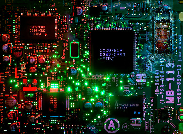
The iconic Moore’s law has guided Silicon Valley and the technology industry at large for over 50 years. Moore’s prediction that the number of transistors on a chip would double every two years (which he first articulated at an ECS meeting in 1964) bolstered businesses and the economy, as well as took society away from the giant mainframes of the 1960s to today’s era of portable electronics.

But research has begun to plateau and keeping up with the pace of Moore’s law has proven to be extremely difficult. Now, many tech-based industries find themselves in a vulnerable position, wondering how far we can push technology.

Better materials, better chips

In an effort to continue Moore’s law and produce the next generation of electronic devices, researchers have begun looking to new materials and potentially even new designs to create smaller, cheaper, and faster chips.

“People keep saying of other semiconductors, ‘This will be the material for the next generation of devices,’” says Fan Ren, professor at the University of Florida and technical editor of the ECS Journal of Solid State Science and Technology. “However, it hasn’t really changed. Silicon is still dominating.”

Silicon has facilitated the growth predicted by Moore’s law for the past decades, but it is now becoming much more difficult to continue that path.

(more…)

Nanostructures

Nanostructures on the surface of the fabric.
Image: Queensland University of Technology

Oil spills have had an extensive history of disrupting the environment, killing ecosystems, and displacing families. Impacts of massive oil spills are still felt in many parts of the world, including the undersea spill at the BP oil rig in the Gulf of Mexico that dumped an approximate 39 million gallons of oil into the gulf.

But what if these devastating oil spills could be easily cleaned up with a piece of fabric rooted in electrochemistry?

That may be a reality soon thanks to researchers at Queensland University of Technology (QUT). According to a release, the QUT researchers have developed a multipurpose fabric covered with semi-conducting nanostructures that can both mop up oil and degrade organic matter when exposed to light.

(READ: “Superhydrophobic Fabrics for Oil/Water Separation Based on the Metal-Organic Charge-Transfer Complex CuTCNAQ“)

The fabric, which repels water and attracts oil, has already has promising preliminary results. In the early stages of research, the scientists have already been able to mop up crude oil from the surface of both fresh and salt water.

(more…)

The iconic Moore’s law has predicted the technological growth of the chip industry for more than 50 years. When ECS member and co-founder of Intel Gordon Moore proposed the law, he stated that the number of transistors on a chip would double every two years. So far, he’s been correct.

But researchers have started hitting an apex that makes keeping the pace of Moore’s law extremely difficult. It has become harder in recent years to make transistors smaller while simultaneously increasing the processing power of chips, making it almost impossible to continue Moore’s law’s projected growth.

However, researchers from MIT have developed a long-awaited tool that may be able to keep driving that progress.

(READ: “Moore’s Law and the Future of Solid-State Electronics“)

The new technology that hopes to keep Moore’s law going at its current pace is called extreme-ultraviolet (EUV) lithography. Industry leaders say it could be used in high-volume chip manufacturing as early as 2018, allowing continued growth in the semiconductor industry, with advancements in our mobile phones, wearable electronics, and many other gadgets.

(more…)

Helping Medicine with Graphene Quantum Dots

Researchers from the University of Sydney have recently published their findings that quantum dots made of graphene can improve bio-imaging and LEDs.

The study was published in the journal Nanoscale, where the scientists detailed how activating graphene quantum dots produced a dot that would shine nearly five times bright than the conventional equivalent.

Essentially, the dots are nano-sized semiconductors, which are fluorescent due to their surface properties. However, this study introduces the utilization of graphene in the quantum dot, which produces an extra-bright dot that has the potential to help medicine.

(more…)

The ECS Journal of Solid State Science and Technology (JSS) is one of the newest peer-reviewed journals from ECS launched in 2012.

The ECS Journal of Solid State Science and Technology (JSS) is one of the newest peer-reviewed journals from ECS launched in 2012.

Printing technologies in an atmospheric environment offer the potential for low-cost and materials-efficient alternatives for manufacturing electronics and energy devices such as luminescent displays, thin film transistors, sensors, thin film photovoltaics, fuel cells, capacitors, and batteries.

This focus issue will cover state-of-the-art efforts that address a variety of approaches to printable functional materials and devices.

Topics of interest include but are not limited to:

  • Printable functional materials: metals; organic conductors; organic and inorganic semiconductors; and more
  • Functional printed devices: RFID tags and antenna; thin film transistors; solar cells; and more
  • Advances in printing and conversion processes: ink chemistry; ink rheology; printing and drying process; and more
  • Advances in conventional and emerging printing techniques: inkjet printing; aerosol printing; flexographic printing; and more

Find out more!

Deadline for submission of manuscripts is November 30, 2014.

Please submit manuscripts here.

ECS Connections to 2014 Physics Nobel Prize

The 2014 Nobel Prize in Physics has been awarded to Shuji Nakamura, a professor at the University of California

Shuji Nakamura, the recipient of the 2014 Nobel Prize in Physics and former ECS Plenary speaker, is awarded for his invention of efficient blue light-emitting diodes.
Credit: Randall Lamb

The 2014 Nobel Prize in Physics has been awarded to Shuji Nakamura, professor of materials and of electrical and computer engineering at the University of California and 2010 ECS Plenary speaker.

The prize is for the invention of efficient blue light-emitting diodes, which has enabled bright and energy-saving white light sources, and is shared with ECS member Isamu Akasaki of Meijo University and Nagoya University, Japan; and Hiroshi Amano of Nagoya University.

In his plenary talk at the 218th ECS Meeting in Las Vegas, Nevada, Nakamura described the current status of III-nitride based light emitting diodes (LEDs) and laser diodes. Nitride-based white LEDs have been used for many application such as LCD TV backlight, lighting for inside/outside applications and others.

According to the Royal Swedish Academy of Sciences, when Nakamura, Akasaki and Amono “produced bright blue light beams from their semiconductors in the early 1990s, they triggered a fundamental transformation of lighting technology. Red and green diodes had been around for a long time, but without blue light, white lamps could not be created. Despite considerable efforts, both in the scientific community and in industry, the blue LED had remained a challenge for three decades.”

The LED lamp “holds great promise for increasing the quality of life for over 1.5 billion people around the world who lack access to electricity grids,” the academy continued.

Here’s a list of articles in the ECS Digital Library written by the 2014 Physics Nobel Prize Winners. You can look at them for free:

Hiroshi Amano and Isamu Akasaki

Widegap Column-III Nitride Semiconductors for UV/Blue Light Emitting Devices

Growth and Luminescence Properties of Mg-Doped GaN Prepared by MOVPE

Isamu Akasaki

Epitaxial Growth and Properties of AIxGal.xN by MOVPE

Etching Characteristics and Light Figures of the {111} Surfaces of GaAs

Shuji Nakamura

Piezoelectric Field in Semi-Polar InGaN/GaN Quantum Wells

Read more about Shuji Nakamura’s plenary talk.

Read more about 2014 Nobel Prize winners for Physics.

  • Page 1 of 2
    • 1
    • 2