JSS Editors’ Choice article discusses AlGaN/GaN HEMTs

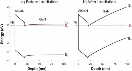
When it comes to putting technology in space, size and mass are prime considerations. High-power gallium nitride-based high electron mobility transistors (HEMTs) are appealing in this regard because they have the potential to replace bulkier, less efficient transistors, and are also more tolerant of the harsh radiation environment of space. Compared to similar aluminum gallium arsenide/gallium arsenide HEMTs, the gallium nitride-based HEMTs are ten times more tolerant of radiation-induced displacement damage.

Until recently, scientists could only guess why this phenomena occurred: Was the gallium nitride material system itself so inherently disordered that adding more defects had scant effect? Or did the strong binding of gallium and nitrogen atoms to their lattice sites render the atoms more difficult to displace?

The answer, according to scientists at the Naval Research Laboratory, is none of the above.

Examining radiation response

In a recent open access article published in the ECS Journal of Solid State Science and Technology entitled, “On the Radiation Tolerance of AlGaN/GaN HEMTs,” the team of researchers from NRL state that by studying the effect of proton irradiation on gallium nitride-based HEMTs with a wide range of initial threading dislocation defectiveness, they found that the pre-irradiation material quality had no effect on radiation response.

Additionally, the team discovered that the order-of-magnitude difference in radiation tolerance between gallium arsenide- and gallium nitride-based HEMTs is much too large to be explained by differences in binding energy. Instead, they noticed that radiation-induced disorder causes the carrier mobility to decrease and the scattering rate to increase as expected, but the carrier concentration remains significantly less affected than it should be.

(more…)

From televisions screens we can roll up like newspapers to see-through batteries, researchers are moving electronics toward a more flexible, more transparent future.

The most recent development in this area comes from a group that has developed transparent, flexible supercapacitors made of carbon nanotube films. But this development goes far beyond wearable electronics, with potential applications in both energy storage and harvesting.

“Potential applications can be roughly divided into two categories: high-aesthetic-value products, such as activity bands and smart clothes, and inherently transparent end-uses, such as displays and windows,” co-author of the study Tanja Kallio, told Phys.org. “The latter include, for example, such future applications as smart windows for automobiles and aerospace vehicles, self-powered rolled-up displays, self-powered wearable optoelectronics, and electronic skin.”

With the thin films demonstrating 92 percent transparency and high efficiency compared to other carbon-based counterparts, the researchers believe that further improvements to the supercapacitors durability and energy density could make the product commercially viable.

Nanowire cooling

Flexible electrocaloric fabric of nanowire array can cool.
Image: Qing Wang/Penn State

The utilization of nanowires has opened a new branch of science for many researchers. While some have focused on applying this technology to energy systems, researchers from Penn State are using the nanowires to develop solid state personal cooling systems.

A new study from the university shows that nanowires could help develop a material for lightweight cooling systems, which could be incorporated into firefighting gear, athletic uniforms, and other wearables.

“Most electrocaloric ceramic materials contain lead,” says Qing Wang, professor of materials science and engineering at Penn State. “We try not to use lead. Conventional cooling systems use coolants that can be environmentally problematic as well. Our nanowire array can cool without these problems.”

This from Penn State:

Electrocaloric materials are nanostructured materials that show a reversible temperature change under an applied electric field. Previously available electrocaloric materials were single crystals, bulk ceramics, or ceramic thin films that could cool, but are limited because they are rigid, fragile, and have poor processability. Ferroelectric polymers also can cool, but the electric field needed to induce cooling is above the safety limit for humans.

(more…)

Breakthrough in Polishing of Silicon Carbide

Microscopic interferometric images and slope images of SiC surface (a) before (PV: 23.040 nm, Ra: 1.473 nm, RMS: 1.885 nm) and (b) after (PV: 2.070 nm, Ra: 0.198 nm, RMS: 0.247 nm) polishing with soda-lime glass plate.

Microscopic interferometric images and slope images of SiC surface (a) before (PV: 23.040 nm, Ra: 1.473 nm, RMS: 1.885 nm) and (b) after (PV:
2.070 nm, Ra: 0.198 nm, RMS: 0.247 nm) polishing with soda-lime glass plate.

Guest post by Jennifer Bardwell, Technical Editor of the ECS Journal of Solid State Science and Technology (JSS).

This paper, from Kumamoto University in Japan, concerns a technique for abrasive-free polishing of silicon carbide (SiC). This topic is timely as SiC is an important material for wide bandgap electronics, both in its own right, and as a substrate for gallium nitride electronics. The reviewers note that:

“Defect free polishing of SiC surface has high significance” and that “The results are amazing”

In the words of the abstract: “The experimental results showed that an oxide layer was formed on the SiC surface as a result of the chemical reaction between the interfaces of the synthetic SiO2 glass plate and the SiC substrate. This generated oxide layer was effectively removed by polishing with the soda-lime SiO2 glass plate, resulting in an atomically smooth SiC surface with a root mean square roughness of less than 0.1 nm for 1.5 h. Obtained experimental results indicate that the component materials, temperature and water adsorptive property of the soda-lime SiO2 glass play an important role in the removal of the tribochemically generated layer on the SiC surface during this polishing.”

Read the paper.

Yue Kuo’s work in solid state science has yielded many innovations and has made a tremendous mark on the scientific community. Since his arrival at ECS in 1995, Kuo was named an ECS Fellow, was recently named Vice President of the Society, previously served as an associate editor of the Journal of The Electrochemical Society, and is currently one of the technical editors of the ECS Journal of Solid State Science and Technology. Additionally, Kuo received the ECS Gordon E. Moore Medal for Outstanding Achievement in Solid State Science and Technology at the 227th ECS Meeting.

Listen to the podcast and download this episode and others for free through the iTunes Store, SoundCloud, or our RSS Feed. You can also find us on Stitcher.

(more…)

Analyzing Thin Film Break-Up

The open-source code, WulffMaker, is available as a Wolfram computable document format file or a Mathematica notebook.Image: MIT/Rachel Zucker

The open-source code, WulffMaker, is available as a Wolfram computable document format file or a Mathematica notebook.
Image: MIT/Rachel Zucker

Recent PhD recipient and past ECS student member, Rachel Zucker, examined one of the most complex issues in materials science and has developed a range of mathematical solutions to explain the phenomena known as “dewetting” in solid films. In defense of her thesis, Zucker modeled dewetting in microscale and nanoscale thin films.

Dewetting can be boiled down to the general break-up of material due to excess surface energy. Zucker’s development provides us with not only a new understanding of this phenomenon, but also a way to simulate it. When analyzing solid state dewetting, issues becomes very prominent as engineers attempt to make products with smaller and smaller features.

“The big takeaway is: One, we can write down formulation of this problem; two, we can implement a numerical method to construct the solutions; three, we can make a direct comparison to experiments; and that strikes me as what a thesis should be — the complete thing — formulation, solution, comparison, conclusion,” said W. Craig Carter, MIT professor and Zucker’s co-adviser.

(more…)

Engineers developed this one-material battery by sprinkling carbon (red) into each side of a new material (blue) that forms the electrolyte and both electrodes at the ends of the battery.Source: Maryland NanoCenter

Engineers developed this one-material battery by sprinkling carbon (red) into each side of a new material (blue) that forms the electrolyte and both electrodes at the ends of the battery.
Source: Maryland NanoCenter

ECS student member Fudong Han and former member Chunsheng Wang have developed a novel solid state battery comprised of just one material that can both move and store electricity.

This new battery could prove to be revolutionary in the area of solid state batteries due to its incorporation of electrodes and electrolytes into a single material.

“Our battery is 600 microns thick, about the size of a dime, whereas conventional solid state batteries are thin films — forty times thinner. This means that more energy can be stored in our battery,” said Han, the first author of the paper and a graduate student in Wang’s group.

This from the University of Maryland:

The new material consists of a mix of sulfur, germanium, phosphorus and lithium. This compound is used as the ion-moving electrolyte. At each end, the scientists added carbon to this electrolyte to form electrodes that push the ions back and forth through the electrolyte as the battery charges and discharges. Like a little bit more sugar added at each end of a cookie-cream mixture, the carbon merely helps draw the electricity from side to side through the material.

(more…)

Call for Papers: JSS Focus Issue

focus_issues_coversThe editors of the ECS Journal of Solid State Science and Technology are calling for papers for the upcoming focus issue: Novel Applications of Luminescent Optical Materials.

Submission Deadline: July 15, 2015

Submit your manuscript today!

The research landscape of luminescent and optical materials is rapidly changing due to a need for such materials outside the lighting and display technologies. Novel materials are needed and are developed with luminescent and optical properties appropriately tuned for applications in solar cells, sensors, bio-imaging, light extraction, and related opto-electronics in addition to solid state lighting and display technologies.

Find out more.

Read previous focus issues in ECS journals.

Chemical Reactions Through Brute Force

"Katsenite" named after McGill researcher who analyzed short-lived material’s chemical structure.Source: McGill University

“Katsenite” named after McGill researcher who analyzed short-lived material’s chemical structure.
Source: McGill University

Have you heard of mechanochemistry yet? Researchers from McGill University are making a name for themselves in this up-and-coming multidisciplinary field with their discovery of a new material unveiled through unconventional means.

Prof. Tomislav Friščić’s research group in McGill’s Department of Chemistry is now producing chemical reactions through milling, grinding, or shering solid state ingredients. In other words, the team is using brute force to elicit these reactions rather than the typical liquid agents.

The group states that their process is similar to that of a coffee grinder. The advantage to using force over liquids is that it avoids environmentally harmful bulk solvents that are typically used when producing chemical reactions.

These findings were published in the paper “In Situ X-ray diffraction monitoring of a mechanochemical reaction reveals a unique topology metal-organic framework”. It all began in late 2012, where researchers reported that they had been able to observe milling reaction in real time – seeing chemical transformations using highly penetrating X-rays.

(more…)

Voltage profiles of charge-discharge cycles of the Li/Li3PS4/S battery.Image: Journal of The Electrochemical Society

Voltage profiles of charge-discharge cycles of the Li/Li3PS4/S battery.
Image: Journal of The Electrochemical Society

A team from Japan’s Samsung R&D has worked in collaboration with researchers from the University of Rome to fabricate a novel all solid state Lithium-sulfur battery.

The paper has been recently published in the Journal of The Electrochemical Society. (P.S. It’s Open Access! Read it here.)

The battery’s capacity is around 1,600 mAhg⁻¹, which denotes an initial charge-discharge Coulombic efficiency approaching 99 percent.

Additionally, the battery possesses such beneficial properties as the smooth stripping-deposition of lithium. In contrast to other Li-S cells, the new battery’s activation energy of the charge transfer process is much smaller.

(more…)

  • Page 2 of 4