 The Journal of The Electrochemical Society is publishing a focus issue in connection with the Advances in Organic and Biological Electrochemistry: In Memory of Diane Smith symposium held at the 245th ECS Meeting in San Francisco, CA, from May 26-30, 2024. This focus issue is dedicated to the scientific topics that inspired Diane K. Smith, professor for 30 years in the Department of Chemistry and Biochemistry at San Diego State University.
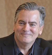
Prof. Smith made significant contributions to teaching and research in electrochemistry. The first woman hired into a tenure track position in her department, her research greatly influenced a variety of electrochemical research topics, including organic electrochemistry, supramolecular chemistry, catalysis, and electrochemical energy storage. She was a renowned mentor for members of our community and an outstanding educator.