A research team, including ECS members Stephen Doorn and Erik H Hároz, has created flexible, wafer-scale films of highly aligned and closely packed carbon nanotubes thanks to a simple filtration process. In a discovery that was previously though impossible, the researchers found that in the right solution and under the right conditions, the tubes can assemble themselves by the millions into long rows.

(ICYMI: Get the freshman 101 on carbon nanotubes from nanocarbons expert Bruce Weisman.)

This development could help bring flexible electronics to actuality, especially with the special electronic properties of the nanotubes.

“Once we have centimeter-sized crystals consisting of single-chirality nanotubes, that’s it,” said Junichiro Kono, Rice University physicist leading the study. “That’s the holy grail for this field. For the last 20 years, people have been looking for this.”

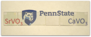
penn-state-materialA new material developed at Penn State could mean big things for everything from smartphones to solar cells.

For over 60 years, the main material used in transparent conductor display has been indium tin oxide. With over 90 percent of the display market utilizing this material, it has left very little room for competitor materials.

While indium tin oxide has provided solid efficiency levels at a decent price point for the past half decades, expenses have recently skyrocketed on this material.

Current electronic devices, such as smart phones and tables, are primarily priced according to display material costs. Displays and touch screen modules make up 40 percent of the cost to produce a device, greatly outpacing other essential pieces such as chips and processors. It hasn’t been until now that researchers have found a material that could potential replace indium tin oxide and potentially reduce device costs.

(more…)

Building Better Electronic Devices

The development of the silicon chip forever changed the field of electronics and the world at large. From computers to cellphones to digital home appliances, the silicon chip has become an inextricable part of the structure of our society. However, as silicon begins to reach its limits many researchers are looking for new materials to continue the electronics revolution.

Fan Ren, Distinguished Professor at the University of Florida and Technical Editor of the ECS Journal of Solid State Science and Technology, has based his career in the field of electronics and semiconductor devices. From his time at Bell Labs through today, Ren has witnessed much change in the field.

Future of Electronics

Upon coming to the United States from Taiwan, Ren was hired by Bell Labs. This hub of innovation had a major impact on Ren and his work, and is where he first got his hands-on semiconductor research. During this time, silicon was the major player as far as electronic materials went. While electronics have transformed since that time, the materials used to create integrated circuits have essentially stayed the same.

People keep saying of other semiconductors, “This will be the material for the next generation of devices,” says Ren. “However, it hasn’t really changed. Silicon is still dominating.”

(more…)

Developing Carbon Nanotube Transistors

carbon_nanotubesx519Since the development of the transistor in 1947, the semiconductor industry has been working to rapidly and continuously improve performance and processing speeds of computer chips. Following Gordon Moore’s iconic law—stating that transistor density would double every two years—the semiconducting silicon chip has propelled technology through a wave of electronic transformation.

Next Electronics Revolution

But all good things must come to an end. The process of packing silicon transistors onto computer chips is reaching its physical limits. However, IBM researchers state that they’ve made a “major engineering breakthrough” that provides a viable alternative to silicon transistors.

The team from IBM proposes using carbon nanotube transistors as an alternative, which have promising electrical and thermal properties. In theory, carbon nanotube transistors could be much faster and more energy efficient than currently used transistors. Nanotube transistors have never been utilized in the past due to major manufacturing challenges that prevented their wide-spread commercialization. However, the IBM researchers are combating this issue by combining the nanotubes with metal contacts to deliver the electrical current.

(more…)

The New iPhone 6S and the Science Behind It

smartphone_homeOnce again, Apple is doing its best to give electronics a huge boost into the future with the release of the new iPhone 6S and iPhone 6S Plus. The technological top dog has upgraded everything from the phone’s processors to its camera—and Apple has finally brought the much anticipated 3D touch capability to life.

While most consumers focus their attention to the phone’s new entertainment abilities and usage innovation, we like to focus on some different aspects here at ECS. While Apple’s Timothy Cook may not have mentioned electrochemistry or solid state science in announcing the new iPhone, these sciences are what allow for higher processing speeds, improved displays, touch recognition, longer battery life, and much more.

Get a full understanding of the science behind the smartphone.

Highlights of the iPhone 6S:

  • Improved 12 megapixel camera
  • Qualocomm chip to double LTE speeds from 150 mbps to 300 mbps
  • Improved TouchID fingerprint sensor
  • New 64-bit chip for 70 percent faster CPU
  • 3D touch capability through sensor technology

Get more info on the iPhone 6S.

PS: Listen to technology and engineering expert Lili Deligianni’s podcast on innovation in electronics!

Power Behind the Next Electronics Revolution

The semiconducting silicon chip brought about a wave of electronic transformation the propelled technology and forever changed the way society functions. We now live in a digital world, where almost everything we encounter on a daily basis is comprised of a mass of silicon integrated circuits (IC) and transistors. But with the materials used to develop and improve these devices being pushed to their limits, the question of the future of electronics arises.

The Beginnings

The move towards a digital age really took flight late in 1947 at Bell Labs when a little device known as the transistor was developed. After this development, Gordon Moore became a pioneering research in the field of electronics and coined Moore’s law in 1965, which dictated that transistor density would double every two years.

Just over 50 years after that prediction, Moore’s law is still holding true. However, researchers and engineers are beginning to hit a bit of a roadblock. Current circuit measurement are coming in a 2nm wide—equating to a size roughly between a red blood cell and a single strand of DNA. Because the integrated circuits are hitting their limit in size, it’s becoming much more difficult to continue the projected growth of Moore’s law.

The question then arises of how do we combat this problem; or do we move toward finding an alternative to silicon itself? What are the true limits of technology?

(more…)

Latest in Flexible Technology

Thanks to a development in OLED (organic light-emitting diode) technology by LG, we can now roll up our television screens like a newspaper.

LG recently unveiled their new 18-inch television panels, which are so flexible they can be rolled up to 3-centemeters without affecting the display or functionality.

The company achieved this through innovation in OLED technology, which allows for thinner, lighter, and more flexible screens. This technology is also lending itself to the second screen LG unveiled, which is nearly transparent.

But why would you want to roll up your television screen? Well, you probably wouldn’t. However, the bendable nature of the panels makes the screens virtually unbreakable and give them the ability to curve to walls to make your viewing experience more aesthetically pleasing.

“LG Display pioneered the OLED TV market and is now leading the next-generation applied OLED technology,” In-Byung Kang, LG Display’s senior vice president and head of the R&D Center, said in a statement. “We are confident that by 2017, we will successfully develop an Ultra HD flexible and transparent OLED panel of more than 60 inches, which will have transmittance of more than 40 percent and a curvature radius of 100R, thereby leading the future display market.”

High-Density Storage, 100 Times Less Energy

Tired of your electronics running out of memory? Rice University’s James Tour and his group of researchers have developed a solid state memory technology that allows for high-density storage while requiring 100 times less energy than traditional designs to operate.

The memory technology has been developed via tantalum oxide, a common insulator in electronics.

This from Futurity:

The discovery by the Rice University lab of chemist James Tour could allow for crossbar array memories that store up to 162 gigabits, much higher than other oxide-based memory systems under investigation by scientists. (Eight bits equal one byte; a 162-gigabit unit would store about 20 gigabytes of information.)

Read the full release here.

James Tour—a past ECS lecturer and pioneer in molecular electronics— and his group at Rice University’s Smalley Institute of Nanoscale Science & Technology are constantly demonstrating the interdisciplinary nature of nano science, and this is no exception. From the development of flexible supercapacitors to using cobalt films for clean fuel production, Tour and his lab are exploring many practical applications where chemistry and nano science intersect.

(more…)

printablelii

The batteries have the ability to be integrated into the surface of the objects, making it seem like seem like there is no battery at all.

A new development out of the Ulsan National Institute of Science and Technology (UNIST) has yielded a new technique that could make it possible to print batteries on any surface.

With recent interests in flexible electronics—such as bendable screen displays—researchers globally have been investing research efforts into developing printable functional materials for both electronic and energy applications. With this, many researchers predict the future of the li-ion battery as one with far less size and shape restrictions, having the ability to be printed in its entirety anywhere.

The research team from UNIST, led by ECS member Sang-Young Lee, is setting that prediction on the track to reality. Their new paper published in the journal Nano Letters details the printable li-ion battery that can exist on almost any surface.

(more…)

Member Spotlight – Chennupati Jagadish

jagadishECS Fellow Chennupati Jagadish has been awarded the IEEE Nanotechnology Pioneer Award for his outstanding contributions to compound semiconductor nanowire and quantum dot optoelectronics.

Dr. Jagadish is a Laureate Fellow and Distinguished Professor at the Australian National University, where he has made major advances in compound semiconductor quantum dot and nanowire growth techniques and optoelectronic devices.

Previously, Dr. Jagadish was awarded the ECS Electronics and Photonics Division Award for his excellence in electronics research outstanding technical contribution to the field of electronics science.

Throughout his scientific career, Dr. Jagadish has published more than 620 research papers—some of which can be found in the Digital Library—and has 5 U.S. patents.

Some of Dr. Jagadish’s current research focuses on nanostructured photovoltaics, which provides novel concepts to produce a more efficient solar cell.

  • Page 3 of 4