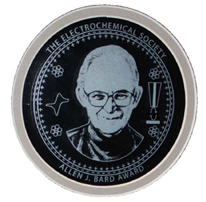
 The Allen J. Bard Award in Electrochemical Science is the most recently-established among the distinguished society-level awards in the ECS Honors and Awards program. If you are an electrochemist, then you know the award’s namesake as the “father of modern electrochemistry.” Many ECS members are a product his Center for Electrochemistry at the University of Texas at Austin.
You now have until June 1 to submit your nomination.
This is a prestigious award that honors innovation in the field. The award winner is recognized for exceptionally creative experimental or theoretical studies that have opened new directions in electroanalytical chemistry or electrocatalysis.
The next award will be conferred at the 235th ECS Meeting in Dallas, TX in May 2019 where the winner will be invited to present the corresponding award talk. In addition, s/he will receive:
- distinctive medallion wall plaque
- $7,500 prize
- complimentary meeting registration
- life membership
- private awards dinner
Read more about the award and previous winners. Check out the handy application tips. And finally, APPLY NOW!