Enzyme-based sensors detect lactate levels in sweat

Sweat Sensor

Image: Sergio Omar Garcia

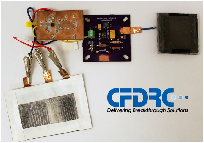
It may be clammy and inconvenient, but human sweat has at least one positive characteristic – it can give insight to what’s happening inside your body. A new study published in the ECS Journal of Solid State Science and Technology aims to take advantage of sweat’s trove of medical information through the development of a sustainable, wearable sensor to detect lactate levels in your perspiration.

“When the human body undergoes strenuous exercise, there’s a point at which aerobic muscle function becomes anaerobic muscle function,” says Jenny Ulyanova, CFD Research Corporation (CFDRC) researcher and co-author of the paper. “At that point, lactate is produce at a faster rate than it is being consumed. When that happens, knowing what those levels are can be an indicator of potentially problematic conditions like muscle fatigue, stress, and dehydration.”

Utilizing green technology

Using sweat to track changes in the body is not a new concept. While there have been many developments in recent years to sense changes in the concentrations of the components of sweat, no purely biological green technology has been used for these devices. The team of CFDRC researchers, in collaboration with the University of New Mexico, developed an enzyme-based sensor powered by a biofuel cell – providing a safe, renewable power source.

Biofuel cells have become a promising technology in the field of energy storage, but still face many issues related to short active lifetimes, low power densities, and low efficiency levels. However, they have several attractive points, including their ability to use renewable fuels like glucose and implement affordable, renewable catalysts.

(more…)

JSS Editors’ Choice article discusses AlGaN/GaN HEMTs

When it comes to putting technology in space, size and mass are prime considerations. High-power gallium nitride-based high electron mobility transistors (HEMTs) are appealing in this regard because they have the potential to replace bulkier, less efficient transistors, and are also more tolerant of the harsh radiation environment of space. Compared to similar aluminum gallium arsenide/gallium arsenide HEMTs, the gallium nitride-based HEMTs are ten times more tolerant of radiation-induced displacement damage.

Until recently, scientists could only guess why this phenomena occurred: Was the gallium nitride material system itself so inherently disordered that adding more defects had scant effect? Or did the strong binding of gallium and nitrogen atoms to their lattice sites render the atoms more difficult to displace?

The answer, according to scientists at the Naval Research Laboratory, is none of the above.

Examining radiation response

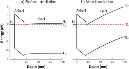
In a recent open access article published in the ECS Journal of Solid State Science and Technology entitled, “On the Radiation Tolerance of AlGaN/GaN HEMTs,” the team of researchers from NRL state that by studying the effect of proton irradiation on gallium nitride-based HEMTs with a wide range of initial threading dislocation defectiveness, they found that the pre-irradiation material quality had no effect on radiation response.

Additionally, the team discovered that the order-of-magnitude difference in radiation tolerance between gallium arsenide- and gallium nitride-based HEMTs is much too large to be explained by differences in binding energy. Instead, they noticed that radiation-induced disorder causes the carrier mobility to decrease and the scattering rate to increase as expected, but the carrier concentration remains significantly less affected than it should be.

(more…)

Call for Papers: 2D Materials

Focus IssuesJSS Technical Editors: Fan Ren and Stefan De Gendt
and
Guest Editors: Lain-Jong (Lance) Li and Daniel S. P. Lau

invite you to submit to the:
JSS Focus Issue:
Properties, Devices, and Applications Based on 2D Layered Materials

Submission Deadline | May 18, 2016

This special issue of the ECS Journal of Solid State Science and Technology focuses on properties, devices, and applications of two-dimensional (2D) based materials including boron nitrides, black phosphorous, transition metal dichalcogenides/oxides, and other layered materials beyond graphene.

Review and contributed papers are welcome in the following domains:

  • Materials preparation
  • Novel growth technology
  • Growth chemistry
  • Metal contacts
  • Surface cleaning and passivation
  • Wet and dry etching
  • Device design and processing integration
  • Device Physics
  • Device and growth simulation
  • Applications of 2D material based devices and systems
  • Heterostructures based on 2D materials

Submission Deadline | May 18, 2016

Please submit manuscripts at http://ecsjournals.msubmit.net

(Be sure to specify your submission is for the JSS Focus Issue on Properties, Devices, and Applications Based on 2D Layered Materials.)

Papers accepted into this focus issue are published online within 10 days of acceptance. The issue is created online an article at a time with the final article published in October 2016.

Breakthrough in Polishing of Silicon Carbide

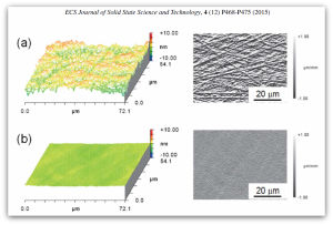
Microscopic interferometric images and slope images of SiC surface (a) before (PV: 23.040 nm, Ra: 1.473 nm, RMS: 1.885 nm) and (b) after (PV: 2.070 nm, Ra: 0.198 nm, RMS: 0.247 nm) polishing with soda-lime glass plate.

Microscopic interferometric images and slope images of SiC surface (a) before (PV: 23.040 nm, Ra: 1.473 nm, RMS: 1.885 nm) and (b) after (PV:
2.070 nm, Ra: 0.198 nm, RMS: 0.247 nm) polishing with soda-lime glass plate.

Guest post by Jennifer Bardwell, Technical Editor of the ECS Journal of Solid State Science and Technology (JSS).
This paper, from Kumamoto University in Japan, concerns a technique for abrasive-free polishing of silicon carbide (SiC). This topic is timely as SiC is an important material for wide bandgap electronics, both in its own right, and as a substrate for gallium nitride electronics. The reviewers note that:

“Defect free polishing of SiC surface has high significance” and that “The results are amazing”

In the words of the abstract: “The experimental results showed that an oxide layer was formed on the SiC surface as a result of the chemical reaction between the interfaces of the synthetic SiO2 glass plate and the SiC substrate. This generated oxide layer was effectively removed by polishing with the soda-lime SiO2 glass plate, resulting in an atomically smooth SiC surface with a root mean square roughness of less than 0.1 nm for 1.5 h. Obtained experimental results indicate that the component materials, temperature and water adsorptive property of the soda-lime SiO2 glass play an important role in the removal of the tribochemically generated layer on the SiC surface during this polishing.”

Read the paper.

Call for Papers: JSS Focus Issue

JSS CoverThis special issue of the ECS Journal of Solid State Science and Technology focuses on defect characterization in semiconductor materials and devices. We especially welcome papers in the following domains:

  • Structural, chemical, electrical and optical characterization of extended defects in semiconductor nano-structures and materials
  • Electrical and optical characterization of point defects in semiconductor nano-structures
  • Semiconductor-device-based defect analysis
  • Impact of (extended) defects on device and circuit operation and yield
  • Defect characterization and control in hetero-epitaxial layers and nano-structures grown on Si, comprising Ge, SiGe, GeSn, III-V and III-nitrides
  • Ab initio calculations and TCAD of the electrical activity of (extended) defects in semiconductor materials and devices
  • Defect control and mitigation strategies during hetero-epitaxial deposition

Find out more!

Submission Deadline | Oct. 21, 2015
Papers accepted into this focus issue are published online within 10 days of acceptance.
The issue is created online an article at a time with the final article published in March 2016.

Call for Nominations

Electronic and Photonic Devices and Systems Technical Editor
for
ECS Journal of Solid State Science and Technology and ECS Solid State Letters

jsssslECS (The Electrochemical Society) is seeking to fill the position of Technical Editor of the Electronic and Photonic Devices and Systems Technical Interest Area for the ECS Journal of Solid State Science and Technology and ECS Solid State Letters.

The Electronic and Photonic Devices and Systems (EPDS) Technical Interest Area (TIA) includes fundamental properties and measurements of device fabrication and characteristics for electronic and photonic applications. Specific topics include thin film transistors; MOSFETs; bipolar devices; quantum devices; silicon, germanium, and related microelectronic and photonic devices; micro- and nano-electro-mechanical systems (MEMS and NEMS); solid state sensors; wide bandgap semiconductor materials and devices; photovoltaic energy conversion devices; phase change memories; graphene-based devices; plasmonics; power devices; silicon-on-insulator devices; and bioelectronics. Learn more.

Call for Papers: JSS Focus Issue

focus_issues_coversThe editors of the ECS Journal of Solid State Science and Technology are calling for papers for the upcoming focus issue: Novel Applications of Luminescent Optical Materials.

Submission Deadline: July 15, 2015

Submit your manuscript today!

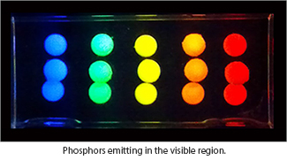
The research landscape of luminescent and optical materials is rapidly changing due to a need for such materials outside the lighting and display technologies. Novel materials are needed and are developed with luminescent and optical properties appropriately tuned for applications in solar cells, sensors, bio-imaging, light extraction, and related opto-electronics in addition to solid state lighting and display technologies.

Find out more.

Read previous focus issues in ECS journals.

The ECS Journal of Solid State Science and Technology (JSS) is one of the newest peer-reviewed journals from ECS launched in 2012.

The ECS Journal of Solid State Science and Technology (JSS) is one of the newest peer-reviewed journals from ECS launched in 2012.

Atomic Layer Etch (ALEt) and Atomic Layer Clean (ALC) are emerging as enabling technologies for sub 10nm technology nodes. At these scales performance will be extremely sensitive to process variation.

Atomic layer processes are the most promising path to deliver the precision needed. However, many areas of ALEt and ALC are in need of improved fundamental understanding and process development. This focus issue will cover state-of-the-art efforts that address a variety of approaches to ALEt and ALC.

Topics of interest include but are not limited to:

  • Surface reaction chemistry and its impact on selectivity
  • Plasma ion energy distribution and control methods
  • Novel plasma sources and potential application to ALEt & ALC
  • Innovative approaches to atomic layer material removal
  • Novel device applications of ALEt & ALC
  • Process chamber design considerations
  • Advanced delivery of chemicals to processing chambers
  • Metrology and control of ALEt & ALC
  • Device performance impact
  • Synthesis of new chemistries for ALEt & ALC application
  • Damage free surface defect removal
  • Process and discharge modeling

Find out more!

Deadline for submission of manuscripts is December 17, 2014.

Please submit manuscripts here.

The ECS Journal of Solid State Science and Technology (JSS) is one of the newest peer-reviewed journals from ECS launched in 2012.

The ECS Journal of Solid State Science and Technology (JSS) is one of the newest peer-reviewed journals from ECS launched in 2012.

Printing technologies in an atmospheric environment offer the potential for low-cost and materials-efficient alternatives for manufacturing electronics and energy devices such as luminescent displays, thin film transistors, sensors, thin film photovoltaics, fuel cells, capacitors, and batteries.

This focus issue will cover state-of-the-art efforts that address a variety of approaches to printable functional materials and devices.

Topics of interest include but are not limited to:

  • Printable functional materials: metals; organic conductors; organic and inorganic semiconductors; and more
  • Functional printed devices: RFID tags and antenna; thin film transistors; solar cells; and more
  • Advances in printing and conversion processes: ink chemistry; ink rheology; printing and drying process; and more
  • Advances in conventional and emerging printing techniques: inkjet printing; aerosol printing; flexographic printing; and more

Find out more!

Deadline for submission of manuscripts is November 30, 2014.

Please submit manuscripts here.

The ECS Journal of Solid State Science and Technology (JSS) is one of the newest peer-reviewed journals from ECS launched in 2012.

The ECS Journal of Solid State Science and Technology (JSS) is one of the newest peer-reviewed journals from ECS launched in 2012.

Atomic Layer Etch (ALEt) and Atomic Layer Clean (ALC) are emerging as enabling technologies for sub 10nm technology nodes. At these scales performance will be extremely sensitive to process variation.

Atomic layer processes are the most promising path to deliver the precision needed. However, many areas of ALEt and ALC are in need of improved fundamental understanding and process development. This focus issue will cover state-of-the-art efforts that address a variety of approaches to ALE and ALC.

Topics of interest include but are not limited to:

  • Surface reaction chemistry and its impact on selectivity
  • Plasma ion energy distribution and control methods
  • Novel plasma sources and potential application to ALEt & ALC
  • Innovative approaches to atomic layer material removal
  • Novel device applications of ALEt & ALC
  • Process chamber design considerations
  • Advanced delivery of chemicals to processing chambers
  • Metrology and control of ALEt & ALC
  • Device performance impact
  • Synthesis of new chemistries for ALEt & ALC application
  • Damage free surface defect removal
  • Process and discharge modeling

Find out more.

  • Page 7 of 7