
ECS is sponsoring the 11th European Space Power Conference, taking place October 3-7, 2016 in Thessaloniki, Greece. The conference, which will focus on electrical power for space applications and cutting-edge research on topics for terrestrial applicators, is currently open for potential presenters to submit their papers.
Following several issues, some related to browsers compatibility and companies systems configuration, we know that some authors were not able to upload their digest. In addition, some digests have not been submitted in the appropriate format as per instructions, being an abstract instead of a digest.
In view of these issues, the ESPC2016 committee has decided to re-open a window: from Friday 22/04/2016 18:00 CET till Monday 25/04/2016 12:00 CET.
Upload your digest before April 22, 2016!
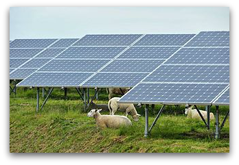
The conference is intended to cover the three main topics of: power generation with solar generators and other types of sources, such as nuclear or electrochemical; energy storage, including batteries and regenerative fuel cells; and power management and distribution, a wide domain covering every level of integration from electrical parts to power subsystem architectures.
If you are not able to login to ESPC2016 digest submission website, the ESPC2016 committee recommends to use another browser.
Learn more about the conference and email espc2016-conference@esa.int for questions or support.
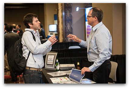 This spring, ECS will be coming to San Diego for our
  This year’s