
 The Directorate for Stem Education of the National Science Foundation (NSF) has announced new award opportunities for FY 2023 and FY 2024 in two programs, Improving Undergraduate STEM Education (IUSE) and Experiential Learning for Emerging and Novel Technologies (ExLENT).T
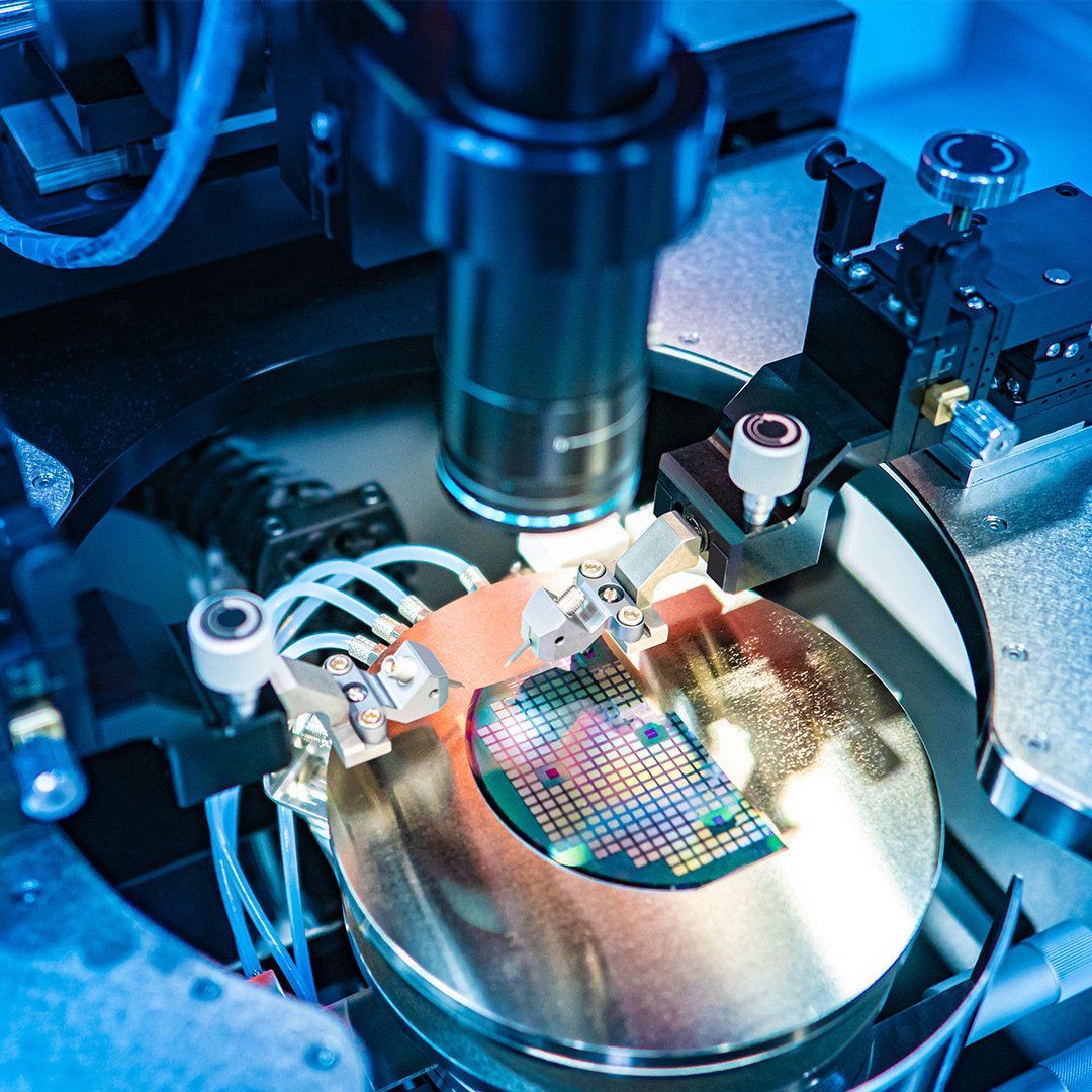
According to the June 13, 2023, “Dear Colleague Letter” (DCL Document number nsf23118), these efforts are intended to build on or leverage strong industry-academic partnerships to strengthen the semiconductor manufacturing workforce by advancing and supporting the development of a skilled STEM workforce in advanced memory manufacturing and/or semiconductor manufacturing and design. The goal is to meet the critical need to expand domestic “semiconductor research and development, design, and manufacturing” and fill the talent shortage in the domestic semiconductor industry through inclusive and equitable STEM education opportunities.

 Deadline Extended: March 19, 2018
 A small metallic tab that, when attached to the body, is capable of generating electricity from bending a finger and other simple movements could one day power our electronic devices.
 For the past four decades, the electronics industry has been driven by what is called “
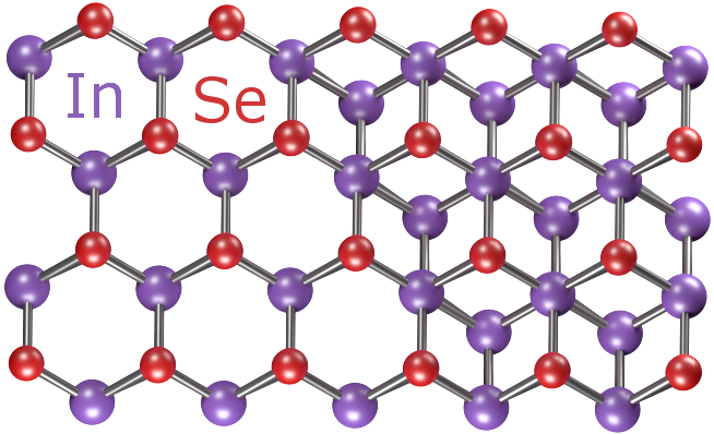 Newly developed semiconductor materials are showing promising potential for the future of super-fast electronics.