Zhichuan (Jason) Xu, PhD, FRSC
Professor
School of Materials Science and Engineering
Nanyang Technological University, Singapore
Date: December 15, 2021
Time: 1000h ET
Sponsor: Hiden Analytical

Zhichuan (Jason) Xu, PhD, FRSC
Professor
School of Materials Science and Engineering
Nanyang Technological University, Singapore
Date: December 15, 2021
Time: 1000h ET
Sponsor: Hiden Analytical
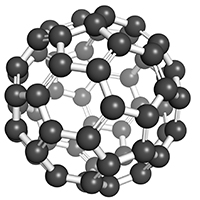 Robert Wong, proprietor of SES Research Inc., is proud to announce a new and exciting materials grant to support researchers whose projects focus on Carbon 60 powder. Through this, researchers can obtain C60—at little or no cost—for their investigations.
 We’ve all been touched by the COVID-19 pandemic in some shape or form and have felt its effects, particularly, within the job market. For job seekers, it’s crucial now more than ever to use all resources at hand to increase visibility and exposure. For employers, having a way to filter through countless job applicants is just as important. The ECS Career Center serves as a source to help you connect and find exactly what you’re for!
The ECS Career Center’s Resume Bank feature allows employers to search resumes in the Resume Bank and target candidates that match the criteria they seek. Job seekers, take advantage of this feature! Use the Upload Your Resume Feature to upload your resume to connect with a potential future employer. (more…)
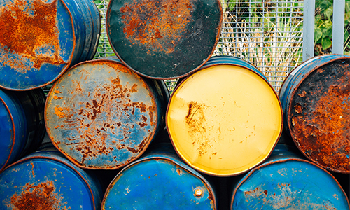 A recent study warns that U.S. nuclear waste storage containers could corrode, according to Ohio State News.
On January 27, in the paper, “Self-accelerated corrosion of nuclear waste forms at material interfaces,” researchers reported that the “corrosion of nuclear waste storage materials accelerates because of changes in the chemistry of the nuclear waste solution, and because of the way the materials interact with one another,” risking harm to people and the surrounding environment. (more…)
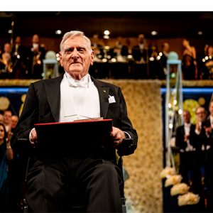
John B. Goodenough © Nobel Media. Photo: Alexander Mahmoud
As John B. Goodenough looked on, his Nobel Lecture was delivered by Arumugam Manthiram at the Aula Magna, Stockholm University, on December 8, 2019. Both Goodenough and Manthiram are fellows of The Electrochemical Society (ECS).
Nobel Laureates are required to give a lecture on a subject connected with the work for which they receive the award. Goodenough videotaped his lecture, “Designing Lithium-ion Battery Cathodes,” before December 8, then invited Manthiram to present it in Stockholm. Manthiram added explanations and comments between Goodenough’s slides and video, concluding with a summary of Goodenough’s research and its historical significance. The three classes of materials Goodenough discovered—layered oxide, spinel oxide, and polyanion oxide—still remain the only viable cathodes and the basis for future development. Goodenough pushed the boundaries of sold-state chemistry and physics. “His trump card is using chemistry and physics to solve engineering problems,” said Manthiram on another occasion. (more…)
 The Electrochemical Society (ECS) is the official sponsor of AEMFC 2019, the Second International Symposium Advances in Anion Exchange Membranes: Materials, Processes and Devices. The symposium takes place on December 7 and 8, 2019, at the Raytheon Amphitheater, Egan Research Center, at Northeastern University in Boston, MA.
“ECS is proud to sponsor AEMFC 2019. These scientists’ research is at the forefront of resolving pressing problems in conservation and more. Meetings like this one, and ECS meetings, are important not only for the information that is shared in the lectures. We believe that in the informal gatherings between meetings, during meals, and in the evenings, connections are made that impact science far into the future,” said Shannon Reed, ECS director of community engagement. (more…)
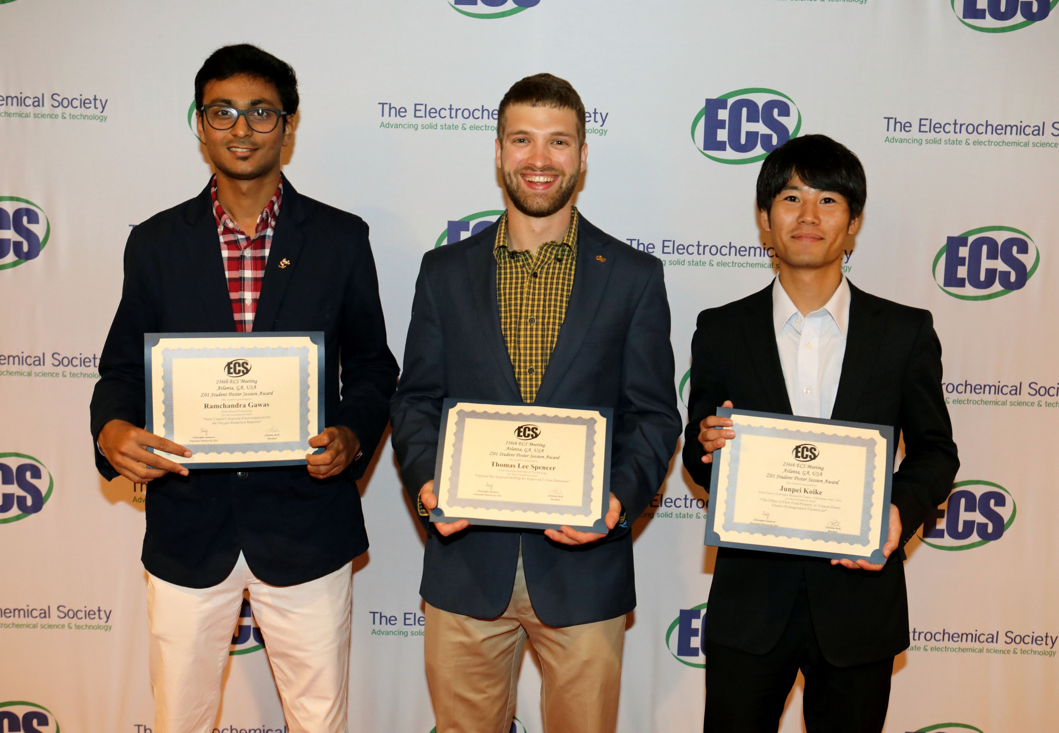
From left to right: Ramchandra Gawas, Thomas Lee Spencer, and Junpei Koike; photo by Robb Cohen Photography and Video
Established in 1993, the General Student Poster Session Awards acknowledge the excellence of students’ work. The winners display their understanding of research topics in fields of interest to The Electrochemical Society (ECS).
This year, at the 236th ECS Meeting in Atlanta, GA, almost 600 students submitted posters to the General Student Poster Session. Of them, three student posters stood out above the rest.
The recipients of the 235th ECS Meeting’s best poster awards are:
1st Place – $1,500 cash award
Ramchandra Gawas, Drexel University
Poster # 2310
“Ionic Liquid Composite Electrocatalysts for the Oxygen Reduction Reaction” (more…)
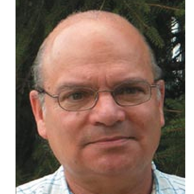 Shimshon Gottesfeld received the 2019 Olin Palladium Award at the 236th Electrochemical Society (ECS) Meeting. The award recognizes distinguished contributions to the field of electrochemical or corrosion science. Gottesfeld talk, “Polymer Electrolyte Fuel Cells: Recognition of a Field of Electrochemistry for Technical Contributions Made by Outstanding Technical Teams,” is on Wednesday, 16 October, at 1640h in Galleria 2.
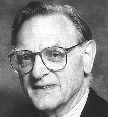
Gottesfeld is an emeritus member and fellow of ECS. He received his PhD in chemistry from Technion – Israel Institute of Technology in Haifa. He joined the staff of the Department of Chemistry at the University of Tel Aviv in 1972. Gottesfeld spent an extended sabbatical leave between 1977 and 1979 at Bell Labs in Murray Hill, New Jersey. In 2015, Gottesfeld was nominated adjunct professor at the Department of Chemical Engineering of the University of Delaware. (more…)
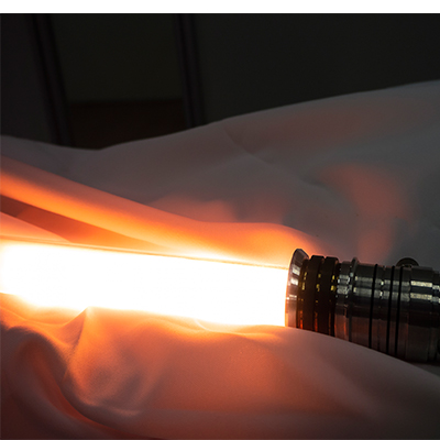 In “The Lightsaber Battery,” author Richard Rogers asks if recent electric vehicle battery research makes a lightsaber battery possible. After reviewing Star Wars technology and the current state of battery technology, his conclusion is a conditional yes! However, the final stage of light saber development depends on a Kyber crystal which amplifies and channels the cosmic energy of the Force. Unfortunately, a crystal like that hasn’t been discovered in our universe yet.
Star Wars fans and electric battery developers do not despair! The need for longer-lasting electric vehicle batteries has raised cycle life goals similar to the lightsaber’s requirements—and electrochemists are rising to the challenge! That galaxy “far, far away” is coming closer and closer. (more…)
John B. Goodenough
Christina Bock, president of the Board of The Electrochemical Society (ECS), congratulated John B. Goodenough, M. Stanley Whittingham, and Akira Yoshino who today were jointly awarded the 2019 Nobel Prize in Chemistry.
“On behalf of the entire ECS community, I would like to extend my sincerest congratulations to our esteemed members: John Goodenough, M. Stanley Whittingham, and Akira Yoshino on being awarded the 2019 Nobel Prize in Chemistry ‘for the development of Lithium-ion batteries,’” said Bock. “This is fitting recognition for the truly groundbreaking advancements these pioneers have made for our field and for the whole of humanity. Simply put, their research is the enabling science upon which the solutions to the grand challenges facing the planet—renewable energy, clean transportation, communications to name but a few—will be based. We are honored to count their almost 60 years of combined membership among our ranks.” (more…)