Throughout the history of the transistor technological revolution, The Electrochemical Society has served as a platform for key inventors to present their research.
In December of 1947—75 years ago—William Shockley, John Bardeen, and Walter Brattain invented the transistor at Bell Telephone Laboratories in New Jersey. The three men shared the 1956 Nobel Prize in Physics “for research on semiconductors and the discovery of the transistor effect.” This invention heralded the modern electronic age. According to science historian Michael Riordan, “[The transistor] has enabled this global civilization. I would put it on the [same] level as fire, in terms of its importance to what modern life is like today.” In a recent ECS Interface article, Hiroshi Iwai and Durga Misra describe the process of the technological development behind the invention of the transistor, and discuss the meaning and impact of its invention on human history.
Shown here is the smallest laptop power adapter ever, made using GaN transistors. Image: Cambridge Electronics
Recent discussions in the electronics industry have revolved around the future of technology in light of the perceived end of Moore’s law. But what if the iconic law doesn’t have to end? Researchers from MIT believe they have exactly what it takes to keep up with the constantly accelerating pace of Moore’s law.
More efficient materials
For the scientists, the trick is in the utilization of a material other than silicon in semiconductors for power electronics. With extremely high efficiency levels that could potentially reduce worldwide energy consumption, some believe that material could be gallium nitride (GaN).
MIT spin-out Cambridge Electronics Inc. (CEI) has recently produced a line of GaN transistors and power electronic circuits. The goal is to cut energy usage in data centers, electric cars, and consumer devices by 10 to 20 percent worldwide by 2025.
Semiconductors shaping society
Since its discovery in 1947, the transistor has helped make possible many wonders of modern life – including smartphones, solar cells, and even airplanes.
Over time, as predicted by Moore’s law, transistors became smaller and more efficient at an accelerated pace – opening doors to even more technological advancements.
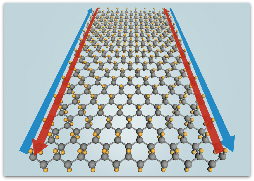
Researchers made a prediction two years ago that a one-atom thick, tin super material would soon be developed. They believed that this mesh material would yield amazing advances for materials science and be able to conduct electricity with 100 percent efficiency. Now, those same researchers are making good on their prediction with the announcement of the newly developed film called stanene.
Theoretically, potential uses of this material could range from circuit structures to transistors.
Cousin to graphene, this lattice of carbon atoms has similar qualities to a host of other materials, but scientists predict stanene to have a special kick that no other material has yet.
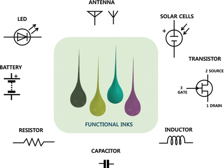
Printing technologies in an atmospheric environment offer the potential for low-cost and materials-efficient alternatives for manufacturing electronics and energy devices such as luminescent displays, thin-film transistors, sensors, thin-film photovoltaics, fuel cells, capacitors, and batteries. Significant progress has been made in the area of printable functional organic and inorganic materials including conductors, semiconductors, and dielectric and luminescent materials.
These new printable functional materials have and will continue to enable exciting advances in printed electronics and energy devices. Some examples are printed amorphous oxide semiconductors, organic conductors and semiconductors, inorganic semiconductor nanomaterials, silicon, chalcogenide semiconductors, ceramics, metals, intercalation compounds, and carbon-based materials.
A special focus issue of the ECS Journal of Solid State Science and Technology was created about the publication of state-of-the-art efforts that address a variety of approaches to printable functional materials and device. This focus issue, consisting of a total of 15 papers, includes both invited and contributed papers reflecting recent achievements in printable functional materials and devices.
The topics of these papers span several key ECS technical areas, including batteries, sensors, fuel cells, carbon nanostructures and devices, electronic and photonic devices, and display materials, devices, and processing. The overall collection of this focus issue covers an impressive scope from fundamental science and engineering of printing process, ink chemistry and ink conversion processes, printed devices, and characterizations to the future outlook for printable functional materials and devices.
The video below demonstrates Printed Metal Oxide Thin-Film Transistors by J. Gorecki, K. Eyerly, C.-H. Choi, and C.-H. Chang, School of Chemical, Biological and Environmental Engineering, Oregon State University.
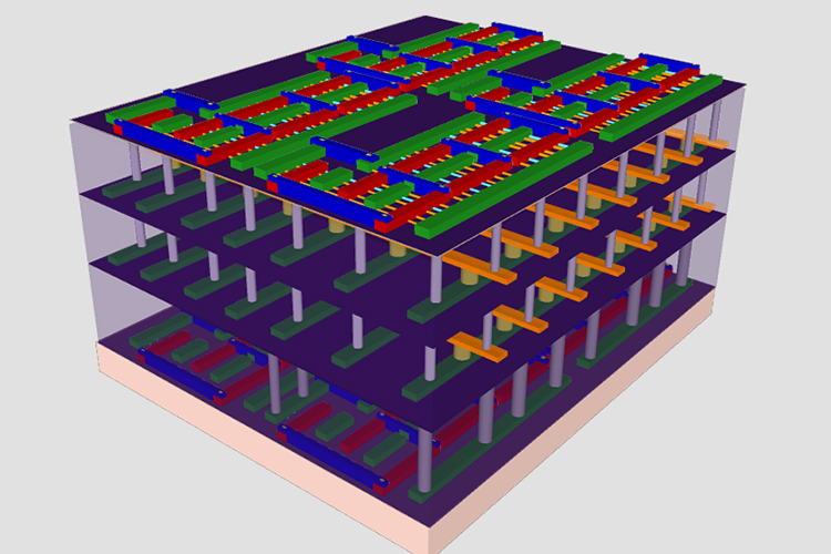
Stanford engineers have created a four-layer prototype high-rise chip. The bottom and top layers are transistors, which are sandwiched between two layers of memory. Credit: Max Shulaker, Stanford
Cheaper, smaller, and faster – those are the three words we’re constantly hearing when it comes to innovation and development in electronics. Now, Stanford University engineers are adding a fourth word to that mantra – taller.
The Stanford team is about to reveal how to build a high-rise chip that could vault the performance of the single-story logic and memory chips on today’s circuit cards – thereby preventing the wires connecting logic and memory from jamming.
This from Stanford University:
The Stanford approach would end these jams by building layers of logic atop layers of memory to create a tightly interconnected high-rise chip. Many thousands of nanoscale electronic “elevators” would move data between the layers much faster, using less electricity, than the bottleneck-prone wires connecting single-story logic and memory chips today.
The ECS Journal of Solid State Science and Technology (JSS) is one of the newest peer-reviewed journals from ECS launched in 2012.
Printing technologies in an atmospheric environment offer the potential for low-cost and materials-efficient alternatives for manufacturing electronics and energy devices such as luminescent displays, thin film transistors, sensors, thin film photovoltaics, fuel cells, capacitors, and batteries.
This focus issue will cover state-of-the-art efforts that address a variety of approaches to printable functional materials and devices.
Topics of interest include but are not limited to:
Printable functional materials: metals; organic conductors; organic and inorganic semiconductors; and more
Functional printed devices: RFID tags and antenna; thin film transistors; solar cells; and more
Advances in printing and conversion processes: ink chemistry; ink rheology; printing and drying process; and more
Advances in conventional and emerging printing techniques: inkjet printing; aerosol printing; flexographic printing; and more
This website uses cookies so that we can provide you with the best user experience possible. Cookie information is stored in your browser and performs functions such as recognising you when you return to our website and helping our team to understand which sections of the website you find most interesting and useful.